


UART Modules
MCF5253 Reference Manual, Rev. 1
15-8
Freescale Semiconductor
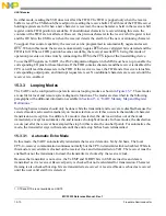
15.3.2.2
Receiver
The receiver is enabled through the UCR located within the UART module. Functional timing information
for the receiver is shown in
. The receiver looks for a high-to-low (mark-to-space) transition
of the start bit on RxD. When a transition is detected the start bit is validated 0.5 baud clock after the
transition. If RxD is sampled high, the start bit is not valid and the search for the valid start bit repeats. If
RxD is still low, a valid start bit is assumed and the receiver continues to sample the input at one-bit time
intervals at the theoretical center of the bit.
Figure 15-6. Receiver Timing Diagram
This process continues until the proper number of data bits and parity (if any) is assembled and one stop
bit is detected. Data on the RxD input is sampled on the rising edge of the programmed clock source. The
least significant bit is received first. The data is then transferred to a receiver holding register and the
RxRDY bit in the USR is set. If the character length is less than eight bits, the most significant unused bits
in the receiver holding register are cleared. The Rx RDY bit in the USR is set at the one-half point of the
stop bit.
After the stop bit is detected, the receiver immediately looks for the next start bit. However, if a nonzero
character is received without a stop bit (framing error) and RxD remains low for one-half of the bit period
after the stop bit is sampled, the receiver operates as if a new start bit is detected. The parity error (PE),
C1
C2
C3
C4
C5
C6
C7
C8
RxD
RECEIVER
ENABLED
C6, C7, C8 ARE LOST DUE TO
RECEIVER DISABLED
RxRDY2(S
RO)
FFULL2.5
(SR1)
R R R R R R
|STATUS DATA| |STATUS DATA| |STATUS
DATA| | | | C2
C3 C4
INTERNAL
MODULE
SELECT CS
R R
|STATUS DATA|
|
OVERRUN
(SR4)
RTS1
(OP0)
RESET BY COMMAND
C5
LOST
NOTES:
1. TIMING SHOWN FOR UMR1[7]=1
2. TIMING SHOWN FOR UMR1[6]=0
3. CN = RECEIVED 5-8 BIT CHARACTER
UOP1[0]=1
R = Read
Summary of Contents for MCF5253
Page 1: ...Document Number MCF5253RM Rev 1 08 2008 MCF5253 Reference Manual...
Page 26: ...MCF5253 Reference Manual Rev 1 xxvi Freescale Semiconductor...
Page 32: ...MCF5253 Reference Manual Rev 1 xxxii Freescale Semiconductor...
Page 46: ...MCF5253 Introduction MCF5253 Reference Manual Rev 1 1 14 Freescale Semiconductor...
Page 62: ...Signal Description MCF5253 Reference Manual Rev 1 2 16 Freescale Semiconductor...
Page 98: ...Instruction Cache MCF5253 Reference Manual Rev 1 5 10 Freescale Semiconductor...
Page 104: ...Static RAM SRAM MCF5253 Reference Manual Rev 1 6 6 Freescale Semiconductor...
Page 128: ...Synchronous DRAM Controller Module MCF5253 Reference Manual Rev 1 7 24 Freescale Semiconductor...
Page 144: ...Bus Operation MCF5253 Reference Manual Rev 1 8 16 Freescale Semiconductor...
Page 176: ...System Integration Module SIM MCF5253 Reference Manual Rev 1 9 32 Freescale Semiconductor...
Page 198: ...Analog to Digital Converter ADC MCF5253 Reference Manual Rev 1 12 6 Freescale Semiconductor...
Page 246: ...DMA Controller MCF5253 Reference Manual Rev 1 14 18 Freescale Semiconductor...
Page 282: ...UART Modules MCF5253 Reference Manual Rev 1 15 36 Freescale Semiconductor...
Page 344: ...Audio Interface Module AIM MCF5253 Reference Manual Rev 1 17 46 Freescale Semiconductor...
Page 362: ...I2 C Modules MCF5253 Reference Manual Rev 1 18 18 Freescale Semiconductor...
Page 370: ...Boot ROM MCF5253 Reference Manual Rev 1 19 8 Freescale Semiconductor...