


System Integration Module (SIM)
MCF5253 Reference Manual, Rev. 1
9-26
Freescale Semiconductor
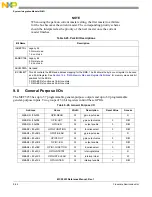
NOTE
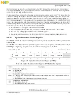
MCLK1 will output a clock signal just after reset and before it can be
configured as a GPIO if so desired. The frequency of the clock will be the
same as CRIN prior to initialization of the PLL.
NOTE
EBUOUT1 will output a clock signal just after reset and before they can be
configured as GPIO. The frequency of the clock output will be CRIN/16.
These two
pins can still be used for GPIO. The user needs to ensure that
when one of these two pins is assigned as a GPIO control within the system,
that its use will not cause the application to exhibit problems when the clock
is active just after reset and before the boot code sets them to GPIO mode,
e.g., do not use these pins to switch a critical circuit on/off.
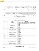
9.8.1.1
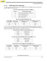
General Purpose Input Interrupts
There are seven general purpose inputs, those associated with GPIO-READ(6:0), have interrupt capability.
On every low-to-high edge transition of these inputs, one of the bits 0–6 of register GPIO-INT-STAT is
set. On every high-to-low edge of the inputs, one of the bits 8–14 is set. Write 1 to clear to the
corresponding bit in GPIO-INT-CLEAR register. If any bit in GPIO-INT-STAT is set, and the
corresponding bit in GPIO-INT-EN is set, an interrupt will be made pending on the secondary interrupt
controller.
NOTE
The registers GPIO-INT-STAT
,
GPIO-INT-CLEAR
and GPIO-INT-EN also
control some audio interrupts.
Set the GPIO_FUNCTION register bit to 1 or 0 for interrupts, as applicable.
GPIO-READ(5)
CFLG/GPIO5
GPIO1-READ(37)
EBUOUT1/GPIO37
GPIO-READ(4)
DDATA3/RTS0/GPIO4
GPIO1-READ(36)
EBUIN1/GPIO36
GPIO-READ(3)
DDATA2/CTSO/GPIO3
GPIO1-READ(35)
SCLK3/GPIO35
GPIO-READ(2)
DDATA1/RTS1/SDATA2_BS2/GPIO2
GPIO1-READ(34)
SDATAO2/GPIO34
GPIO-READ(1)
DDATA0/CTS1/SDATA0_SDIO1/GPIO1
GPIO1-READ(33)
IDE_IORDY/GPIO33
GPIO-READ(0)
XTRIM/TXD2/GPIO0
GPIO1-READ(32)
IDE_DIOW/GPIO32
Table 9-27. General Purpose Input to Pin Mapping (continued)
General
Purpose Input
Read From Pin
General Purpose Input
Read From Pin
Summary of Contents for MCF5253
Page 1: ...Document Number MCF5253RM Rev 1 08 2008 MCF5253 Reference Manual...
Page 26: ...MCF5253 Reference Manual Rev 1 xxvi Freescale Semiconductor...
Page 32: ...MCF5253 Reference Manual Rev 1 xxxii Freescale Semiconductor...
Page 46: ...MCF5253 Introduction MCF5253 Reference Manual Rev 1 1 14 Freescale Semiconductor...
Page 62: ...Signal Description MCF5253 Reference Manual Rev 1 2 16 Freescale Semiconductor...
Page 98: ...Instruction Cache MCF5253 Reference Manual Rev 1 5 10 Freescale Semiconductor...
Page 104: ...Static RAM SRAM MCF5253 Reference Manual Rev 1 6 6 Freescale Semiconductor...
Page 128: ...Synchronous DRAM Controller Module MCF5253 Reference Manual Rev 1 7 24 Freescale Semiconductor...
Page 144: ...Bus Operation MCF5253 Reference Manual Rev 1 8 16 Freescale Semiconductor...
Page 176: ...System Integration Module SIM MCF5253 Reference Manual Rev 1 9 32 Freescale Semiconductor...
Page 198: ...Analog to Digital Converter ADC MCF5253 Reference Manual Rev 1 12 6 Freescale Semiconductor...
Page 246: ...DMA Controller MCF5253 Reference Manual Rev 1 14 18 Freescale Semiconductor...
Page 282: ...UART Modules MCF5253 Reference Manual Rev 1 15 36 Freescale Semiconductor...
Page 344: ...Audio Interface Module AIM MCF5253 Reference Manual Rev 1 17 46 Freescale Semiconductor...
Page 362: ...I2 C Modules MCF5253 Reference Manual Rev 1 18 18 Freescale Semiconductor...
Page 370: ...Boot ROM MCF5253 Reference Manual Rev 1 19 8 Freescale Semiconductor...