


IDE and Flash Media Interface
MCF5253 Reference Manual, Rev. 1
Freescale Semiconductor
13-13
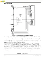
13.5.2
Flash Media Interface Operation
The Flash Media interface is built around two
Interface Shift Registers
, each of which work independently.
shows a block diagram of one interface shift register.
Figure 13-10. Shift Register
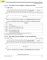
Table 13-9. Flash Media Configuration Register Field Descriptions
Field
Description
Res
31–22
Reserved
–
21–20
CARDTYPE
Card Type
00 Sony Memory Stick
01 SecureDigital, 1-bit serial data
11 SecureDigital, 4-bit serial data
0
19
RECEIVEEDGE
Receive Edge
1
1 Receive data on falling edge of SCLKOUT pin
0 Receive data on rising edge of SCLKOUT pin
1
In SD mode, this bit should be programmed 1. In MemoryStick mode, programming 1 gives more relaxed timing, however
Memory Stick specs stipulate it should be 0.
0
18
Reserved
0
17–16
STOPCLOCK
Stop Clock
00 Normal operation
01 Freeze clock low
10 Freeze clock high
01
15–8
CLOCKCOUNT1
CLOCKCOUNT1+1
is the sclk_out_pin high period in number of bus clocks
15
7–0
CLOCKCOUNT0
CLOC1
2, 3
is the sclk_out_pin low period in number of bus clocks
2
The clock generator will increase the length of some SCLKOUT clock cycles to avoid bus contention when the SDIO pin
switches from input to output, or from output to input mode. The clock generator will stop the SCLKOUT clock if this is
necessary to avoid buffer overrun or buffer underrun.
3
It is acceptable to reprogram these bits while the interface is running. No glitch will occur on sclk_out.
15
Interface
Shift
Register
BS (MemoryStick mode only)
Serial data
CommandBits
bitCounter
shift_busy
int_level
crc_is_0
TxBufferEmpty
RcvBufferFull
loadTxShiftReg
storeRcvShiftReg
stopclock
(to clock generator)
RxBufferFull
Summary of Contents for MCF5253
Page 1: ...Document Number MCF5253RM Rev 1 08 2008 MCF5253 Reference Manual...
Page 26: ...MCF5253 Reference Manual Rev 1 xxvi Freescale Semiconductor...
Page 32: ...MCF5253 Reference Manual Rev 1 xxxii Freescale Semiconductor...
Page 46: ...MCF5253 Introduction MCF5253 Reference Manual Rev 1 1 14 Freescale Semiconductor...
Page 62: ...Signal Description MCF5253 Reference Manual Rev 1 2 16 Freescale Semiconductor...
Page 98: ...Instruction Cache MCF5253 Reference Manual Rev 1 5 10 Freescale Semiconductor...
Page 104: ...Static RAM SRAM MCF5253 Reference Manual Rev 1 6 6 Freescale Semiconductor...
Page 128: ...Synchronous DRAM Controller Module MCF5253 Reference Manual Rev 1 7 24 Freescale Semiconductor...
Page 144: ...Bus Operation MCF5253 Reference Manual Rev 1 8 16 Freescale Semiconductor...
Page 176: ...System Integration Module SIM MCF5253 Reference Manual Rev 1 9 32 Freescale Semiconductor...
Page 198: ...Analog to Digital Converter ADC MCF5253 Reference Manual Rev 1 12 6 Freescale Semiconductor...
Page 246: ...DMA Controller MCF5253 Reference Manual Rev 1 14 18 Freescale Semiconductor...
Page 282: ...UART Modules MCF5253 Reference Manual Rev 1 15 36 Freescale Semiconductor...
Page 344: ...Audio Interface Module AIM MCF5253 Reference Manual Rev 1 17 46 Freescale Semiconductor...
Page 362: ...I2 C Modules MCF5253 Reference Manual Rev 1 18 18 Freescale Semiconductor...
Page 370: ...Boot ROM MCF5253 Reference Manual Rev 1 19 8 Freescale Semiconductor...


