


4-19
BUS PROTOCOL
4.2.1.
Bus Signals
The Request Phase bus signals are ADS#, A[35:3]#, REQa[4:0]#, REQb[4:0]#, ATTR[7:0]#,
DID[7:0]#, BE[7:0]#, EXF[4:0]#, AP[1:0]#, and RP#. In addition, the LOCK# signal is driven
during this phase. Request Phase signals are bused among all agents. Since information is car-
ried during two clocks, the first clock is identified with the suffix a and the second clock is iden-
tified with the suffix b. For example, RPa# and RPb#.
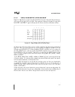
4.2.2.
Request Phase Protocol Description
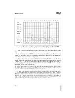
The Request Phase occurs when a transaction is actually issued to the bus. ADS# is asserted
and the transaction information is driven. Figure 4-11 shows the Request Phase of several
transactions.
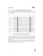
In T1, only one bus agent (agent 0) drives a request for the bus. In T2, BREQ[3:0]#, BPRI# and
BNR# are sampled and it is determined that BREQ0# becomes the bus owner in T3.
In T3, agent 0 drives a transaction by asserting ADS#. Also in T3, A[35:3]#, REQa[4:0]#,
AP[1:0]# and RP# are driven valid. REQa0# indicates that the transaction is a write transaction.
In T4, the second clock of the Request Phase, the rest of the transaction information is driven
out on the following signals: REQb[4:0]#, ATTR[7:0]#, DID[7:0]#, BE[7:0]#, and EXF[4:0]#.
AP[1:0]#, and RP# remain valid in this clock.
When a transaction is driven to the bus, the internal state must be updated in the clock after
ADS# is observed asserted. Therefore, in T5 the internal request count {rcnt} is incremented by
one.
Figure 4-11. Request Generation Phase
CLK
BREQ0#
BPRI#
A[35:3]#
BNR#
ADS#
A
A
AAAAAA
A
AA
AAAAAA
A
AA
AAA
AA
A
AAAA
A
AA
AAAA
AA
A
AAAA
AA
A
AAAA
1
2
3
4
5
6
7
8
9
10
11
12
13
14
15
16
AA
A
AAAAAA
A
AA
AAAAAA
AAAA
AAAA
AAAA
AAAA
AAAA
AAAA
AAAA
AAAA
AAAA
AAAA
AAAA
AAAA
AAAA
AAAA
AAAA
AAAA
AAAA
AAAA
AAAA
AAAA
AAAA
AAAA
AAAA
AAAA
AAAA
AAAA
AAAA
AAAA
AAAA
AAAA
AAAA
AAAA
AAAA
AAAA
AAAA
AAAA
AAAA
AA
A
AAAAAA
A
AA
AAAAAA
A
A
AAA
A
A
AAAAAA
0
0
0
0
1
1
1
2
2
2
7
7
7
7
8
8
REQ[4:0]#
{.rcnt}
Summary of Contents for Pentium Pro Family
Page 17: ...1 Component Introduction ...
Page 26: ...2 Pentium Pro Processor Architecture Overview ...
Page 27: ......
Page 36: ...3 Bus Overview ...
Page 62: ...4 Bus Protocol ...
Page 105: ...5 Bus Transactions and Operations ...
Page 126: ...6 Range Registers ...
Page 131: ...7 Cache Protocol ...
Page 135: ...8 Data Integrity ...
Page 148: ...9 Configuration ...
Page 161: ...10 Pentium Pro Processor Test Access Port TAP ...
Page 172: ...11 Electrical Specifications ...
Page 201: ...12 GTL Interface Specification ...
Page 229: ...13 3 3V Tolerant Signal Quality Specifications ...
Page 233: ...14 Thermal Specifications ...
Page 239: ...15 Mechanical Specifications ...
Page 241: ...15 2 MECHANICAL SPECIFICATIONS s Figure 15 1 Package Dimensions Bottom View ...
Page 252: ...16 Tools ...
Page 260: ...16 8 TOOLS Figure 16 4 Generic MP System Layout for Debug Port Connection ...
Page 264: ...17 OverDrive Processor Socket Specification ...
Page 290: ...A Signals Reference ...
Page 320: ...Index ...
Page 328: ......