


11-9
ELECTRICAL SPECIFICATIONS
11.8.
SIGNAL GROUPS
In order to simplify the following discussion, signals have been combined into groups by buffer
type. All outputs are open drain and require an external hi-level source provided externally by
the termination or a pull-up resistor.
GTL+ input signals have differential input buffers which use VREF as their reference signal.
GTL+ output signals require termination to 1.5V. Later in this document, the term “GTL+ Input”
refers to the GTL+ input group as well as the GTL+ I/O group when receiving. Similarly,
“GTL+ Output” refers to the GTL+ output group as well as the GTL+ I/O group when driving.
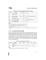
The 3.3V tolerant, Clock, APIC and JTAG inputs can each be driven from ground to 3.3V. The
3.3V tolerant, APIC, and JTAG outputs can each be pulled high to as much as 3.3V. See Table
11-7 for specifications.
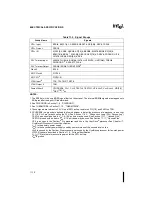
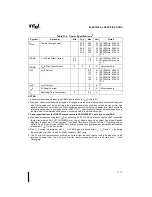
The groups and the signals contained within each group are shown in Table 11-2. Note that the
signals ASZ[1:0]#, ATTR[7:0]#, BE[7:0]#, BREQ#[3:0], DEN#, DID[7:0]#, DSZ[1:0]#,
EXF[4:0]#, LEN[1:0]#, SMMEM#, and SPLCK# are all GTL+ signals that are shared onto an-
other pin. Therefore they do not appear in this table.
11.8.1.
Asynchronous vs. Synchronous
All GTL+ signals are synchronous. All of the 3.3V tolerant signals can be applied asyn-
chronously, except when running two processors in FRC mode. To run in FRC mode,
synchronization logic is required on all signals, except PWRGOOD, going to both processors.
Also note the timing requirements for PICCLK with respect to BCLK. With FRC enabled, PIC-
CLK must be ¼X BCLK and synchronized with respect to BCLK with PICCLK lagging BCLK
by at least 1 ns and no more than 5 ns.
Summary of Contents for Pentium Pro Family
Page 17: ...1 Component Introduction ...
Page 26: ...2 Pentium Pro Processor Architecture Overview ...
Page 27: ......
Page 36: ...3 Bus Overview ...
Page 62: ...4 Bus Protocol ...
Page 105: ...5 Bus Transactions and Operations ...
Page 126: ...6 Range Registers ...
Page 131: ...7 Cache Protocol ...
Page 135: ...8 Data Integrity ...
Page 148: ...9 Configuration ...
Page 161: ...10 Pentium Pro Processor Test Access Port TAP ...
Page 172: ...11 Electrical Specifications ...
Page 201: ...12 GTL Interface Specification ...
Page 229: ...13 3 3V Tolerant Signal Quality Specifications ...
Page 233: ...14 Thermal Specifications ...
Page 239: ...15 Mechanical Specifications ...
Page 241: ...15 2 MECHANICAL SPECIFICATIONS s Figure 15 1 Package Dimensions Bottom View ...
Page 252: ...16 Tools ...
Page 260: ...16 8 TOOLS Figure 16 4 Generic MP System Layout for Debug Port Connection ...
Page 264: ...17 OverDrive Processor Socket Specification ...
Page 290: ...A Signals Reference ...
Page 320: ...Index ...
Page 328: ......