


11-25
ELECTRICAL SPECIFICATIONS
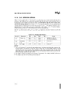
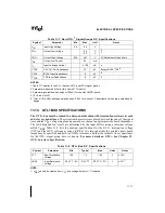
Figure 11-9. Setup and Hold Timings
Ts
= Setup Time
Th
= Hold Time
V
= 1.0V for GTL+ signal group; 1.5V for 3.3V Tolerant, APIC and JTAG signal groups
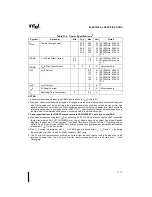
Figure 11-10. Lo to Hi GTL+ Receiver Ringback Tolerance
The Hi to Low Case is analogous.
α
=
Overshoot
τ
=
Minimum Time at High
ρ
=
Amplitude of Ringback
φ
=
Final Settling Voltage
V
REF
+ 0.2
V
REF
−
0.2
Time
V
REF
Clock
1.5 V Clk Ref
V
start
τ
0
.3
--
0
.8
V
/ns
−ρ
T
su
+0.05ns
φ
α
Summary of Contents for Pentium Pro Family
Page 17: ...1 Component Introduction ...
Page 26: ...2 Pentium Pro Processor Architecture Overview ...
Page 27: ......
Page 36: ...3 Bus Overview ...
Page 62: ...4 Bus Protocol ...
Page 105: ...5 Bus Transactions and Operations ...
Page 126: ...6 Range Registers ...
Page 131: ...7 Cache Protocol ...
Page 135: ...8 Data Integrity ...
Page 148: ...9 Configuration ...
Page 161: ...10 Pentium Pro Processor Test Access Port TAP ...
Page 172: ...11 Electrical Specifications ...
Page 201: ...12 GTL Interface Specification ...
Page 229: ...13 3 3V Tolerant Signal Quality Specifications ...
Page 233: ...14 Thermal Specifications ...
Page 239: ...15 Mechanical Specifications ...
Page 241: ...15 2 MECHANICAL SPECIFICATIONS s Figure 15 1 Package Dimensions Bottom View ...
Page 252: ...16 Tools ...
Page 260: ...16 8 TOOLS Figure 16 4 Generic MP System Layout for Debug Port Connection ...
Page 264: ...17 OverDrive Processor Socket Specification ...
Page 290: ...A Signals Reference ...
Page 320: ...Index ...
Page 328: ......