


11-20
ELECTRICAL SPECIFICATIONS
NOTE:
1. Specified for an edge rate of 0.3-0.8V/ns. See Section 12.1.3.1., “Ringback Tolerance” for the definition of
these terms. See Figure 12-3 and Figure 12-4 for the generic waveforms. All values determined by
design/characterization.
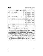
NOTES:
1. Valid delay timings for these signals are specified into 150
Ω
to 3.3V. See Figure 11-6 for a capacitive der-
ating curve.
2. These inputs may be driven asynchronously. However, to guarantee recognition on a specific clock, the
setup and hold times with respect to BCLK must be met.
3. These signals must be driven synchronously in FRC mode.
4. A20M#, IGNNE#, INIT# and FLUSH# can be asynchronous inputs, but to guarantee recognition of these
signals following a synchronizing instruction such as an I/O write instruction, they must be valid with
active RS[2:0]# signals of the corresponding synchronizing bus transaction.
5. INTR and NMI are only valid in APIC disable mode. LINT[1:0]# are only valid in APIC enabled mode.
6. When driven inactive, or after Power, VREF, BCLK, and the ratio signals are stable.
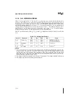
Table 11-12. GTL+ Signal Groups Ringback Tolerance
T#
Parameter
Min
Unit
Figure
Notes
α
:
Overshoot
0.55
mV
11-10
1
τ
:
Minimum Time at High
1.5
ns
11-10
1
ρ
:
Amplitude of Ringback
-100
mV
11-10
1
δ
:
Duration of Squarewave Ringback
N/A
ns
11-10
1
φ
:
Final Settling Voltage
100
mV
11-10
1
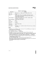
Table 11-13. 3.3V Tolerant Signal Groups A.C. Specifications
T# Parameter
Min
Max
Unit
Figure
Notes
T11:
3.3V Tolerant Output Valid Delay
1
8
ns
11-8
1
T12: 3.3V Tolerant Input Setup Time
5
ns
11-9
2, 3, 4, 5
T13: 3.3V Tolerant Input Hold Time
1.5
ns
11-9
T14: 3.3V Tolerant Input Pulse Width,
except PWRGOOD
2
BCLKs
11-8
Active and
Inactive states
T15: PWRGOOD Inactive Pulse Width
10
BCLKs
11-8
11-13
6
Summary of Contents for Pentium Pro Family
Page 17: ...1 Component Introduction ...
Page 26: ...2 Pentium Pro Processor Architecture Overview ...
Page 27: ......
Page 36: ...3 Bus Overview ...
Page 62: ...4 Bus Protocol ...
Page 105: ...5 Bus Transactions and Operations ...
Page 126: ...6 Range Registers ...
Page 131: ...7 Cache Protocol ...
Page 135: ...8 Data Integrity ...
Page 148: ...9 Configuration ...
Page 161: ...10 Pentium Pro Processor Test Access Port TAP ...
Page 172: ...11 Electrical Specifications ...
Page 201: ...12 GTL Interface Specification ...
Page 229: ...13 3 3V Tolerant Signal Quality Specifications ...
Page 233: ...14 Thermal Specifications ...
Page 239: ...15 Mechanical Specifications ...
Page 241: ...15 2 MECHANICAL SPECIFICATIONS s Figure 15 1 Package Dimensions Bottom View ...
Page 252: ...16 Tools ...
Page 260: ...16 8 TOOLS Figure 16 4 Generic MP System Layout for Debug Port Connection ...
Page 264: ...17 OverDrive Processor Socket Specification ...
Page 290: ...A Signals Reference ...
Page 320: ...Index ...
Page 328: ......