


5-19
BUS TRANSACTIONS AND OPERATIONS
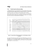
Before T9, the addressed response agent obtains the data required in the original request. In T9,
the original response agent issues a Deferred Reply Transaction, using the value latched from
the DID[7:0]# signals in the original transaction as the address. In T13, the response agent drives
a valid level on the HIT# signal to indicate the final cache state of the returned line. The original
requestor picks up snoop responsibility. In T15, it drives normal completion response and also
begins the Data Phase.
In T10, the original requesting agent observes the Deferred Reply Transaction. It matches the
DID[7:0]# to the Deferred ID stored with the original request in its outstanding transaction
queue. The original requesting agent observes the final state of the returned cache line in T14.
In T16, it observes the transaction response and removes the transaction from the outstanding
transaction queue and the In-order Queue. This completes the entire deferred operation
sequence.
5.3.4.
Locked Operations
Locked operations provide a means of synchronization in a multiprocessor environment. They
guarantee indivisible sequencing between multiple memory transactions.
A locked instruction is guaranteed to lock the area of memory defined by the destination oper-
and. In addition, a lock’s integrity is not affected by the memory operand’s alignment.
In previous generation processors, lock semantics were implemented with a [split] bus lock. This
approach, although sufficient to guarantee indivisibility, is not always necessary or efficient in a
writeback caching agent. During bus lock, other agents are prevented from issuing bus transac-
tions. In multiprocessing systems, it is desirable to reduce the data bus bandwidth demands of
locked operations, so the Pentium Pro processor implements cache locks. Cache locks allow
locked operations to take place in the cache without tying up the bus.
A locked operation in the Intel386 and Intel486 architecture involves an indivisible read-
modify-write operation on the lock variable. Based on the memory type and alignment of the
lock variable, a locked operation is carried out using one of three options:
Cache Lock. When the lock variable is in a writeback-cacheable (WB) memory range and the
lock variable is contained in one cache line, the locked operation can be executed by:
1) executing any bus transactions necessary to bring the line into the Exclusive or Modified
cache state, and 2) executing the locked read-modify-write sequence in the cache, placing the
line in the Modified state.
[Split] Bus Lock. When the lock variable cannot use a cache lock (due to attribute conflicts) or
crosses an 8-byte boundary, the locked operation is issued on the Pentium Pro processor bus. The
bus is locked during the entire read-modify-write sequence to guarantee indivisibility.
Some implementations might use a bus lock or split lock even when a cache lock is allowed.
Summary of Contents for Pentium Pro Family
Page 17: ...1 Component Introduction ...
Page 26: ...2 Pentium Pro Processor Architecture Overview ...
Page 27: ......
Page 36: ...3 Bus Overview ...
Page 62: ...4 Bus Protocol ...
Page 105: ...5 Bus Transactions and Operations ...
Page 126: ...6 Range Registers ...
Page 131: ...7 Cache Protocol ...
Page 135: ...8 Data Integrity ...
Page 148: ...9 Configuration ...
Page 161: ...10 Pentium Pro Processor Test Access Port TAP ...
Page 172: ...11 Electrical Specifications ...
Page 201: ...12 GTL Interface Specification ...
Page 229: ...13 3 3V Tolerant Signal Quality Specifications ...
Page 233: ...14 Thermal Specifications ...
Page 239: ...15 Mechanical Specifications ...
Page 241: ...15 2 MECHANICAL SPECIFICATIONS s Figure 15 1 Package Dimensions Bottom View ...
Page 252: ...16 Tools ...
Page 260: ...16 8 TOOLS Figure 16 4 Generic MP System Layout for Debug Port Connection ...
Page 264: ...17 OverDrive Processor Socket Specification ...
Page 290: ...A Signals Reference ...
Page 320: ...Index ...
Page 328: ......