


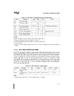


11-5
ELECTRICAL SPECIFICATIONS
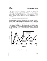
11.5.
BCLK CLOCK INPUT GUIDELINES
The BCLK input directly controls the operating speed of the GTL+ bus interface. All GTL+ ex-
ternal timing parameters are specified with respect to the rising edge of the BCLK input. Clock
multiplying within the processor is provided by an internal Phase Lock Loop (PLL) which re-
quires a constant frequency BCLK input. Therefore the BCLK frequency cannot be changed dy-
namically. It can however be changed when RESET# is active assuming that all reset
specifications are met for the clock and the configuration signals.
The Pentium Pro processor core frequency must be configured during reset by using the A20M#,
IGNNE#, LINT1/NMI, and LINT0/INTR pins. The value on these pins during RESET#, and un-
til two clocks beyond the end of the RESET# pulse, determines the multiplier that the PLL will
use for the internal core clock. See the Appendix A for the definition of these pins during reset.
At all other times their functionality is defined as the compatibility signals that the pins are
named after. These signals are 3.3V tolerant so that they may be driven by existing logic devices.
This is important for both functions of the pins.
Supplying a bus clock multiplier this way is required in order to increase processor performance
without changing the processor design, and to maintain the bus frequency such that system
boards can be designed to function properly as CPU frequencies increase.
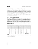
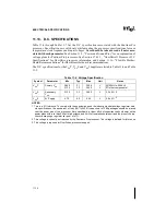
11.5.1.
Setting the Core Clock to Bus Clock Ratio
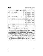
Table 9-4 lists the configuration pins and the values that must be driven at reset time in order to
set the core clock to bus clock ratio. Figure 11-3 shows the timing relationship required for the
clock ratio signals with respect to RESET# and BCLK. CRESET# from an 82453GX is shown
since its timing is useful for controlling the multiplexing function that is required for sharing the
pins.
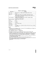
Figure 11-3. Timing Diagram of Clock Ratio Signals
CRESET#
Final
Ratio
Compatibility
BCLK
RESET#
Ratio pins#
≤
Final
Ratio
Summary of Contents for Pentium Pro Family
Page 17: ...1 Component Introduction ...
Page 26: ...2 Pentium Pro Processor Architecture Overview ...
Page 27: ......
Page 36: ...3 Bus Overview ...
Page 62: ...4 Bus Protocol ...
Page 105: ...5 Bus Transactions and Operations ...
Page 126: ...6 Range Registers ...
Page 131: ...7 Cache Protocol ...
Page 135: ...8 Data Integrity ...
Page 148: ...9 Configuration ...
Page 161: ...10 Pentium Pro Processor Test Access Port TAP ...
Page 172: ...11 Electrical Specifications ...
Page 201: ...12 GTL Interface Specification ...
Page 229: ...13 3 3V Tolerant Signal Quality Specifications ...
Page 233: ...14 Thermal Specifications ...
Page 239: ...15 Mechanical Specifications ...
Page 241: ...15 2 MECHANICAL SPECIFICATIONS s Figure 15 1 Package Dimensions Bottom View ...
Page 252: ...16 Tools ...
Page 260: ...16 8 TOOLS Figure 16 4 Generic MP System Layout for Debug Port Connection ...
Page 264: ...17 OverDrive Processor Socket Specification ...
Page 290: ...A Signals Reference ...
Page 320: ...Index ...
Page 328: ......