


10-4
PENTIUM® PRO PROCESSOR TEST ACCESS PORT (TAP)
•
Exit2-DR: This is a temporary state. All registers retain their previous values.
•
Update-DR: Data from the shift register path is loaded into the latched parallel outputs of
the selected Data Register (if applicable) on the falling edge of TCK. This (and Test-Logic-
Reset) is the only state in which the latched paralleled outputs of a data register can
change.
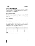
10.2.1.
Accessing the Instruction Register
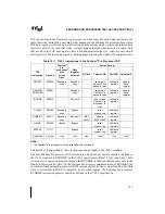
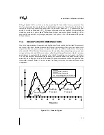
Figure 10-3 shows the (simplified) physical implementation of the Pentium Pro processor TAP
instruction register. This register consists of a 6-bit shift register (connected between TDI and
TDO), and the actual instruction register (which is loaded in parallel from the shift register). The
parallel output of the TAP instruction register goes to the TAP instruction decoder, shown in
Figure 10-1. This architecture conforms to the 1149.1 specification.
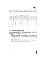
Figure 10-4 shows the operation of the TAP instruction register during the Capture-IR, Shift-IR
and Update-IR states of the TAP controller. Flip-flops within the instruction register which are
updated in each mode of operation are shaded. In Capture-IR, the shift register portion of the
instruction register is loaded in parallel with the fixed value “000001.” In Shift-IR, the shift reg-
ister portion of the instruction register forms a serial data path between TDI and TDO. In Up-
date-IR, the shift register contents are latched in parallel into the actual instruction register. Note
that the only time the outputs of the actual instruction register change is during Update-IR.
Therefore, a new instruction shifted into the Pentium Pro processor TAP does not take effect un-
til the Update-IR state of the TAP controller is entered.
Figure 10-3. Pentium
®
Pro Processor TAP instruction Register
AAAAAAAAAAAAAAAAAAAAAAAAAAAAAAAAAAAAAAAAAAAAAAAAAAAAAAAAAA
AA
AA
AA
AA
AA
AA
AA
AA
AA
AA
AA
AA
AA
AA
AA
AA
AA
AA
AA
AA
AA
AA
AA
AA
AA
AA
AA
AA
AA
AA
AA
AA
AA
AA
AA
AA
AA
AAAAAAAAAAAAAAAAAAAAAAAAAAAAAAAAAAAAAAAAAAAAAAAAAAAAAAAAA
A
A
A
A
A
A
A
A
A
A
A
A
A
A
A
A
A
A
A
A
A
A
A
A
A
A
A
A
A
A
A
A
A
A
A
A
A
TDI
Shift Register
Actual Instruction Register
(LSB)
(MSB)
Parallel output
Fixed capture value
TDO
Summary of Contents for Pentium Pro Family
Page 17: ...1 Component Introduction ...
Page 26: ...2 Pentium Pro Processor Architecture Overview ...
Page 27: ......
Page 36: ...3 Bus Overview ...
Page 62: ...4 Bus Protocol ...
Page 105: ...5 Bus Transactions and Operations ...
Page 126: ...6 Range Registers ...
Page 131: ...7 Cache Protocol ...
Page 135: ...8 Data Integrity ...
Page 148: ...9 Configuration ...
Page 161: ...10 Pentium Pro Processor Test Access Port TAP ...
Page 172: ...11 Electrical Specifications ...
Page 201: ...12 GTL Interface Specification ...
Page 229: ...13 3 3V Tolerant Signal Quality Specifications ...
Page 233: ...14 Thermal Specifications ...
Page 239: ...15 Mechanical Specifications ...
Page 241: ...15 2 MECHANICAL SPECIFICATIONS s Figure 15 1 Package Dimensions Bottom View ...
Page 252: ...16 Tools ...
Page 260: ...16 8 TOOLS Figure 16 4 Generic MP System Layout for Debug Port Connection ...
Page 264: ...17 OverDrive Processor Socket Specification ...
Page 290: ...A Signals Reference ...
Page 320: ...Index ...
Page 328: ......