


9-9
CONFIGURATION
9.2.
CLOCK FREQUENCIES AND RATIOS
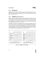
The Pentium Pro processor bus and Pentium Pro processor use a ratio clock design, in which the
bus clock is multiplied by a ratio to produce the processor’s internal (or “core”) clock. The Pen-
tium Pro processor begins sampling A20M# and IGNNE# on the inactive-to-active transition of
RESET# to determine the core-frequency to bus-frequency relationship and immediately begins
the internal PLL lock mode. On the active-to-inactive transition of RESET#, the Pentium Pro
processor internally latches the inputs to allow the pins to be used for normal functionality. Ef-
fectively, these pins must meet a large setup time (1ms) to the active-to-inactive transition
of RESET#.
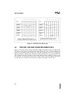
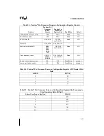
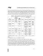
Table 9-4 describes the relationship between bus frequency and core frequency. See Figure
11-10 for a list of tested ratios per product.
NOTE:
1. L and H designate electrical levels.
NOTES
If the power-on configuration information supplied on the two pins is the
same for all CPUs on the Pentium Pro processor bus, the CPUs will run with
identical core frequency. The system designer has the flexibility to operate
different CPUs at different core frequencies by supplying a different ratio to
individual CPU pins.
Intel may also introduce different bus frequency to core frequency ratios than
the ones currently specified. In order to introduce ratios other than 2, 3, and 4,
two additional configuration pins, LINT[1:0], are currently reserved.
Table 9-4. Bus Frequency to Core Frequency Ratio Configuration1
Ratio of Core
Freq to Bus Freq
LINT[1]
LINT[0]
IGNNE#
A20M#
2
L
L
L
L
3
L
L
H
L
4
L
L
L
H
Reserved
L
L
H
H
5/2
L
H
L
L
7/2
L
H
H
L
Reserved
L
H
L
H
Reserved
L
H
H
H
Reserved
HLLL - HHHL
2
H
H
H
H
Summary of Contents for Pentium Pro Family
Page 17: ...1 Component Introduction ...
Page 26: ...2 Pentium Pro Processor Architecture Overview ...
Page 27: ......
Page 36: ...3 Bus Overview ...
Page 62: ...4 Bus Protocol ...
Page 105: ...5 Bus Transactions and Operations ...
Page 126: ...6 Range Registers ...
Page 131: ...7 Cache Protocol ...
Page 135: ...8 Data Integrity ...
Page 148: ...9 Configuration ...
Page 161: ...10 Pentium Pro Processor Test Access Port TAP ...
Page 172: ...11 Electrical Specifications ...
Page 201: ...12 GTL Interface Specification ...
Page 229: ...13 3 3V Tolerant Signal Quality Specifications ...
Page 233: ...14 Thermal Specifications ...
Page 239: ...15 Mechanical Specifications ...
Page 241: ...15 2 MECHANICAL SPECIFICATIONS s Figure 15 1 Package Dimensions Bottom View ...
Page 252: ...16 Tools ...
Page 260: ...16 8 TOOLS Figure 16 4 Generic MP System Layout for Debug Port Connection ...
Page 264: ...17 OverDrive Processor Socket Specification ...
Page 290: ...A Signals Reference ...
Page 320: ...Index ...
Page 328: ......