


5-16
BUS TRANSACTIONS AND OPERATIONS
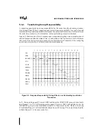
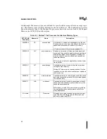
In T5, P1 observes request 2 and notes that the request is to the same cache line for which it is
expecting ownership in T6. In T6, P1 observes inactive DEFER# and confirms that the transac-
tion has been committed for in-order completion.
If P1 changes the state of the cache line to M (as opposed to E/I), then P1 asserts HITM# in T8
to indicate that it has the cache line in the Modified state. In T8, P1 receives a successful com-
pletion response for request 1. P1 recognizes that it has promised the cache line to a different
agent. It completes its internal cache line update and gets ready to return the line to P2.
In T9, the memory agent observes HITM# and asserts TRDY# in T10 in response to the HITM#.
In response in T12, the memory agent asserts implicit writeback response and P1 asserts DB-
SY#. From T12 to T15, P1 drives the implicit cache line data on the data bus. Agent P2 recog-
nizes that the Read Invalidate request is given an implicit writeback response. It receives the new
data associated with the cache line, updates its cache line, and then resumes operation.
Similar to this example, when an Invalidate Line Transaction receives a deferred response, the
corresponding Deferred Reply Transaction may or may not contain data depending on the race
condition. If the Deferred Reply Transaction does not contain data, the deferred reply agent as-
serts a No Data Response. If the Deferred Reply Transaction contains data, the deferred reply
agent asserts HITM# in the Snoop Phase of the Deferred Reply Transaction and asserts an Im-
plicit Writeback response. The original request initiator recognizes that a modified cache line is
being returned and receives the new cache line and updates its internal storage. Memory is not
updated with the Implicit Writeback data of a Deferred Reply Transaction.
5.3.3.
Deferred Operations
During the Request Phase, an agent can define Defer Enable (DEN#) to indicate if the transac-
tion can be given Deferred Response.
When the flag is inactive, the transaction must not receive a Deferred Response. Certain trans-
actions must always be issued with the flag inactive. Transactions in a bus-locked operation, De-
ferred Reply transactions, and Writeback transactions fall in this category. Transaction-latency
sensitive agents may also use this feature to guarantee transaction completion within a restricted
latency. In-order completion of a transaction is indicated by an inactive DEFER# signal or an
active HITM# signal during the Snoop Phase, followed by normal completion or implicit write-
back response in the Response Phase.
When Defer Enable (DEN#) is inactive, the transaction may be completed in-order or possibly
retried, but it cannot be deferred. All transactions may be completed in order. The only transac-
tions that may not be retried are explicit writeback transactions (REQa[2:0]# = 101B) and locked
transactions subsequent to the first transaction in a locked sequence. The retry feature is avail-
able for use by any bus agent incapable of supporting Deferred Response. These transactions
may either be completed in-order (DEFER# inactive or HITM# active during the Snoop Phase
followed by normal completion response), or they must be retried (DEFER# active and HITM#
inactive during the Snoop Phase followed by a Retry Response during the Response Phase).
When Defer Enable (DEN#) is active, the transaction may be completed in-order, or it may be
retried or deferred. A deferred transaction is indicated by asserting DEFER# (with HITM# in-
active) during the Snoop Phase followed by Deferred Response in the Response Phase.
Summary of Contents for Pentium Pro Family
Page 17: ...1 Component Introduction ...
Page 26: ...2 Pentium Pro Processor Architecture Overview ...
Page 27: ......
Page 36: ...3 Bus Overview ...
Page 62: ...4 Bus Protocol ...
Page 105: ...5 Bus Transactions and Operations ...
Page 126: ...6 Range Registers ...
Page 131: ...7 Cache Protocol ...
Page 135: ...8 Data Integrity ...
Page 148: ...9 Configuration ...
Page 161: ...10 Pentium Pro Processor Test Access Port TAP ...
Page 172: ...11 Electrical Specifications ...
Page 201: ...12 GTL Interface Specification ...
Page 229: ...13 3 3V Tolerant Signal Quality Specifications ...
Page 233: ...14 Thermal Specifications ...
Page 239: ...15 Mechanical Specifications ...
Page 241: ...15 2 MECHANICAL SPECIFICATIONS s Figure 15 1 Package Dimensions Bottom View ...
Page 252: ...16 Tools ...
Page 260: ...16 8 TOOLS Figure 16 4 Generic MP System Layout for Debug Port Connection ...
Page 264: ...17 OverDrive Processor Socket Specification ...
Page 290: ...A Signals Reference ...
Page 320: ...Index ...
Page 328: ......