


and the power supply will turn off.
3.4.3 Current Programming
Current programming, like voltage programming, does not require the voltage reference at
terminal 21 of JS1. To produce the voltage reference, a current source is applied to a shunt
resistor. Using a 2 mA current source, place a 10.0 K precision metal film resistor between
terminals 1 and 3 of JS1. The input impedance between terminals 1 and 3 is 10K and paralleling
the additional resistor produces an equivalent resistance of 5K. The 2 mA current source will
produce 10.0 V at the external voltage reference input which will produce full scale output
voltage.
The current set point, over voltage trip, and over current trip can be programmed in the same
manner. Referring to the Table 3.1 for terminal identification, use terminal 22 to program the
current set point, terminal 4 to program over voltage trip, and terminal 23 to program over
current trip. The power supply has been calibrated to produce full scale output voltage and
current with 10.0 V inputs at the external reference input terminals. Furthermore, over voltage
and over current trip have been calibrated to trip at 110% full scale output voltage and current
with 10.0 V inputs at the external reference input terminals.
If the applied voltage at any input is greater than 12.50 V, the pgl (program line) LED will light
and the power supply will turn off.
3.5
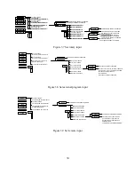
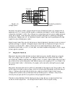
Voltage and Current Monitoring
Two outputs are provided for monitoring output voltage and current and for use in master/slave
series and parallel operation. As illustrated in figure 3.14, output monitoring voltage, VO2, can
be obtained by monitoring the voltage between terminals terminal 5 of JS1 and terminal 1,2 or
20 of JS1. Output monitoring current, IO2, can be obtained by monitoring the voltage between
terminals terminal 24 of JS1 and terminal 1,2 or 20 of JS1. Like the programming inputs, full
scale output voltage and current will produce 10.0 V. The output impedance at these terminals is
100
Ω
.
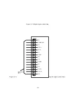
3.6
Digital Input and Output Lines
All digital input and output control lines are connected to connector JS1 located on the rear
panel. As illustrated in figure 3.15, the digital input lines are start, stop, clear, and interlock set.
Functionally, the digital input control lines emulate the functions on the front panel when
external control is enabled. Enabling external control and external interlock is described in
Section 3.1.3.
38
Summary of Contents for XR III series
Page 1: ...OPERATING AND SERVICE MANUAL XR SERIES III DC POWER SUPPLIES...
Page 2: ......
Page 3: ...MAGNA POWER ELECTRONICS INC 39 ROYAL ROAD FLEMINGTON NJ 08822 February 20 2012...
Page 4: ......
Page 88: ...Figure 4 1 Status Byte Generation Figure 4 2 ESE and ESR Generation 76...
Page 95: ...IEEE Standard CLS ESR ESE STB SRE IDN SAV RCL RST Notes 1 C command Q query 83...
Page 97: ...Figure 5 1 Configuration setup Figure 5 2 GPIB communications setup 85...
Page 99: ...Figure 5 4 Virtual Control Panel Figure 5 5 Command Panel 87...
Page 102: ...Figure 5 7 Calibration Panel Figure 5 8 Firmware Panel 90...
Page 103: ...Figure 5 9 Modulation Panel 91...
Page 123: ...Figure B 1 Information Panel Figure B 2 Configure Panel 111...
Page 124: ...Figure B 3 Reboot in Progress Panel Figure B 4 Web Control Panel 112...


