FR200 Series Vector control inverter
- 97 -
1: Negative logic; ON when no current passes through
0: Positive logic; ON when there is coil excitation
1: Negative logic; ON when there is no coil excitation
Wiring diagram of digital output terminal is shown as Fig. 6-12:
24V
Y1
GND
Relay
Inverter
Fig. 6-12
F05.09
Detection width of
frequency attained
Range:0.0
~
20.0Hz
Default:5.0Hz
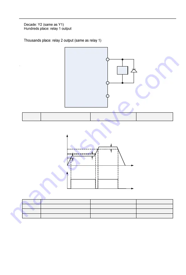
This parameter should be set with digital output terminal "frequency attained". When the
difference between output frequency and command frequency is less than this value, terminal
"frequency attained" aoutputs ON. See Fig. 6-13:
Valid
FAR
FAR
Output frequency(Hz)
Time
(
S
)
Time
(
S
)
Valid
Fig. 6-13
F05.10
FDT1 upper bound
Range:0.00
~
Fmax
Default:30.00Hz
F05.11
FDT1 lower bound
Range:0.00
~
Fmax
Default:30.00Hz
F05.12
FDT2 upper bound
Range:0.00
~
Fmax
Default:30.00Hz
F05.13
FDT2 lower bound
Range:0.00
~
Fmax
Default:30.00Hz
These parameters should be set with digital output terminals "FDT1" and "FDT2".
Take FDT1 for example, the drive outputs ON signal when output frequency exceeds upper
bound of FDT1 and will not output OFF signal unless output frequency drops to below lower bound of
FDT1. Please set F05.10 to be larger to some certain extent than F05.11, avoiding status change
frequently. See Fig. 6-14:


