9
© 2008 - 2011 TOSHIBA TEC CORPORATION All rights reserved
e-STUDIO2020C/2330C/2820C/2830C/3520C/3530C/4520C
POWER SUPPLY UNIT
9 - 3
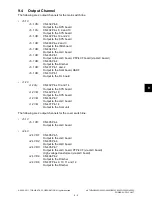
9.4
Output Channel
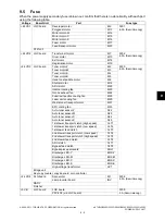
The following are 2 output channels for the main switch line.
•
+5.1 V
+5.1 VS:
CN402 Pin 6
Output to the SYS board
+5.1 VA:
CN402 Pins 8, 9 and 10
Output to the SYS board
+5.1 VB:
CN402 Pins 19 and 20
Output to the SYS board
+5.1 VB:
CN403 Pins 2 and 3
Output to the IMG board
+5.1 VB:
CN404 Pin 1
Output to the LGC board
+5.1 VB:
CN405 Pin 1
Output to the LGC board, PFP/LCF board (via LGC board)
+5.1 VB:
CN406 Pin 4
Output to the Finisher
+5.1 VB:
CN407 Pin 1 and 2
Output to the SLG board, RADF
+5.1 VB:
CN410 Pin 1
Output to the FIL board
•
+12 V
+12 VA:
CN402 Pins 13 and 14
Output to the SYS board
+12 VB:
CN402 Pin 18
Output to the SYS board
+12 VB:
CN404 Pin 7
Output to the LGC board
+12 VB:
CN407 Pin 14
Output to the SLG unit
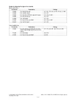
The following are 2 output channels for the cover switch line.
•
+5.1 V
+5.1 VD:
CN405 Pin 4
Output to the LGC board
•
+24 V
+24 VD1:
CN405 Pin 5
Output to the LGC board
+24 VD2:
CN405 Pin 6
Output to the LGC board
+24 VD3:
CN405 Pin 7
Output to the LGC board, PFP/LCF (via LGC board)
High-voltage transformer (via LGC board)
+24 VD4:
CN406 Pin 2
Output to the Finisher
+24 VD4:
CN407 Pins 9, 10, 11 and 12
Output to the Finisher

