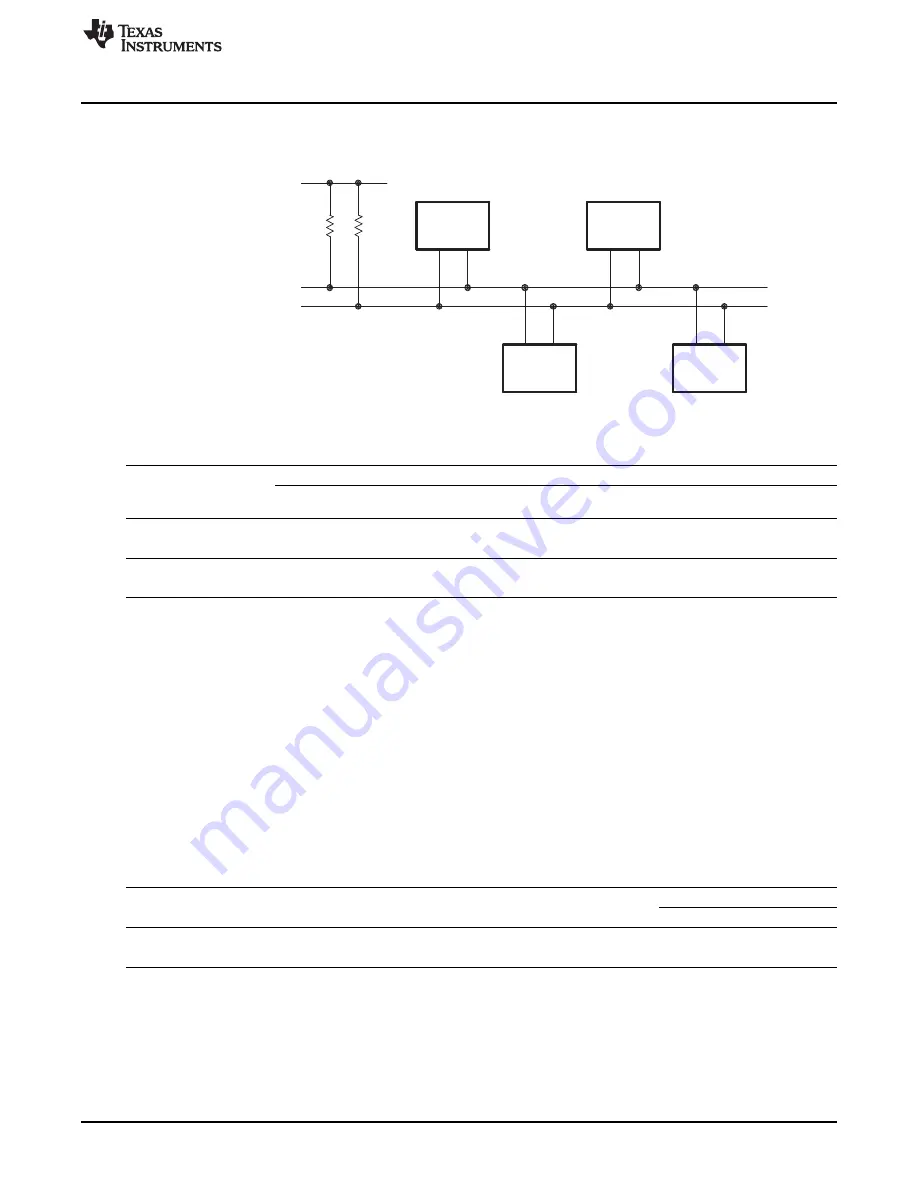
TI device
I2C
I
2
C
EPROM
I
2
C
I2C
TI device
V
DD
Pull-up
resistors
Serial data (I2Cx_SDA)
Serial clock (I2Cx_SCL)
controller
Functional Description
Figure 21-4. Multiple I2C Modules Connected
Table 21-6. Signal Pads
I2C Mode
Default Operating
Name
Mode
Description
I2C_SCL
In/ Out
I2C serial CLK line
Open-drain output buffer. Requires external pull-up resistor (Rp).
I2C_SDA
In/ Out
I2C serial data line
Open-drain output buffer. Requires external pull-up resistor (Rp).
21.3.3 I2C Reset
The I2C module can be reset in the following three ways:
•
A system reset (PIRSTNA = 0). A device reset causes the system reset. All registers are reset to
power up reset values.
•
A software reset by setting the SRST bit in the I2C_SYSC register. This bit has exactly the same
action on the module logic as the system bus reset. All registers are reset to power up reset values.
•
The I2C_EN bit in the I2C_CON register can be used to hold the I2C module in reset. When the
system bus reset is removed (PIRSTNA = 1), I2C_EN = 0 keeps the functional part of I2C module in
reset state and all configuration registers can be accessed. I2C_EN = 0 does not reset the registers to
power up reset values.
Table 21-7. Reset State of I2C Signals
I2C Reset
Pin
I/O/Z
(1)
System Reset
(I2C_EN = 0)
SDA
I/O/Z
High impedance
High impedance
SCL
I/O/Z
High impedance
High impedance
(1)
I = Input, O = Outpu, Z = High impedance
21.3.4 Data Validity
The data on the SDA line must be stable during the high period of the clock. The high and low states of
the data line can only change when the clock signal on the SCL line is LOW.
3703
SPRUH73H – October 2011 – Revised April 2013
I2C
Copyright © 2011–2013, Texas Instruments Incorporated


