ST STM32L4 5 Series Скачать руководство пользователя страница 1345

DocID024597 Rev 5

1345/1830

RM0351

Universal synchronous asynchronous receiver transmitter (USART)

1411

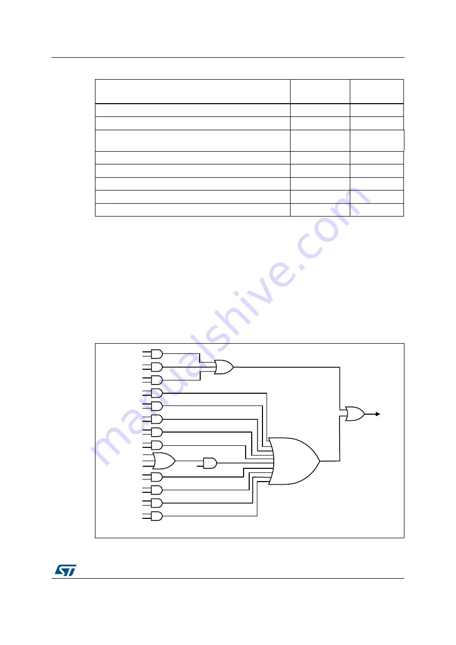
The USART interrupt events are connected to the same interrupt vector (see 

Figure 430

).

During transmission: Transmission Complete, Transmission complete before guard 
time, Clear to Send, Transmit data Register empty or Framing error (in Smartcard 
mode) interrupt.

During reception: Idle Line detection, Overrun error, Receive data register not empty, 
Parity error, LIN break detection, Noise Flag, Framing Error, Character match, etc.

These events generate an interrupt if the corresponding Enable Control Bit is set.

Figure 430. USART interrupt mapping diagram  

Parity error

PE

PEIE

LIN break

LBDF

LBDIE

Noise Flag, Overrun error and Framing Error in multibuffer 
communication.

NF or ORE or FE

EIE

Character match 

CMF

CMIE

Receiver timeout

RTOF

RTOIE

End of Block 

EOBF

EOBIE

Wakeup from Stop mode

WUF

(1)

WUFIE

Transmission complete before guard time

(2)

TCBGT

TCBGTIE

1. The WUF interrupt is active only in Stop mode.

2. Available on STM32L496xx/4A6xx devices only. 

Table 239. USART interrupt requests (continued)

Interrupt event

Event flag

Enable Control 

bit

06Y9

7&

7&,(

7;(

7;(,(

&76,)

&76,(

,'/(

,'/(,(

5;1(,(

25(

5;1(,(

5;1(

3(

3(,(

/%')

/%',(

&0)

&0,(

(2%)

(2%,(

:8)

:8),(

)(

1)

25(

572)

572,(

(,(

86$57

LQWHUUXSW

Содержание STM32L4 5 Series

Страница 1: ...rocontrollers with different memory sizes packages and peripherals For ordering information mechanical and electrical device characteristics please refer to the corresponding datasheets For informatio...

Страница 2: ...ntroduction 72 2 2 2 Memory map and register boundary addresses 75 2 3 Bit banding 83 2 4 Embedded SRAM 84 2 4 1 SRAM2 Parity check 84 2 4 2 SRAM2 Write protection 85 2 4 3 SRAM2 Read protection 87 2...

Страница 3: ...KEYR 122 3 7 3 Flash key register FLASH_KEYR 123 3 7 4 Flash option key register FLASH_OPTKEYR 123 3 7 5 Flash status register FLASH_SR 124 3 7 6 Flash control register FLASH_CR 125 3 7 7 Flash ECC re...

Страница 4: ...atile data segment length FW_VDSL 146 4 4 7 Configuration register FW_CR 147 4 4 8 Firewall register map 149 5 Power control PWR 150 5 1 Power supplies 150 5 1 1 Independent analog peripherals supply...

Страница 5: ...n control register PWR_PDCRB 189 5 4 12 Power Port C pull up control register PWR_PUCRC 189 5 4 13 Power Port C pull down control register PWR_PDCRC 190 5 4 14 Power Port D pull up control register PW...

Страница 6: ...4 6 2 17 Clock out capability 214 6 2 18 Internal external clock measurement with TIM15 TIM16 TIM17 215 6 2 19 Peripheral clock enable register RCC_AHBxENR RCC_APBxENRy 217 6 3 Low power modes 218 6 4...

Страница 7: ...B3 peripheral clocks enable in Sleep and Stop modes register RCC_AHB3SMENR 259 6 4 25 APB1 peripheral clocks enable in Sleep and Stop modes register 1 RCC_APB1SMENR1 259 6 4 26 APB1 peripheral clocks...

Страница 8: ...twise handling 294 8 3 6 GPIO locking mechanism 295 8 3 7 I O alternate function input output 295 8 3 8 External interrupt wakeup lines 295 8 3 9 Input configuration 295 8 3 10 Output configuration 29...

Страница 9: ...register 1 SYSCFG_EXTICR1 312 9 2 4 SYSCFG external interrupt configuration register 2 SYSCFG_EXTICR2 314 9 2 5 SYSCFG external interrupt configuration register 3 SYSCFG_EXTICR3 315 9 2 6 SYSCFG exter...

Страница 10: ...2 331 10 3 13 From comparators COMP1 COMP2 to timers TIM1 TIM2 TIM3 TIM8 TIM15 TIM16 TIM17 331 10 3 14 From system errors to timers TIM1 TIM8 TIM15 TIM16 TIM17 332 10 3 15 From timers TIM16 TIM17 to I...

Страница 11: ...and background FIFOs 359 12 3 4 DMA2D foreground and background pixel format converter PFC 360 12 3 5 DMA2D foreground and background CLUT interface 362 12 3 6 DMA2D blender 363 12 3 7 DMA2D output PF...

Страница 12: ...ine register DMA2D_NLR 386 12 5 19 DMA2D line watermark register DMA2D_LWR 387 12 5 20 DMA2D AHB master timer configuration register DMA2D_AMTCR 387 12 5 21 DMA2D IP version register DMA2D_VERR 387 12...

Страница 13: ...1 Software interrupt event register 2 EXTI_SWIER2 407 14 5 12 Pending register 2 EXTI_PR2 408 14 5 13 EXTI register map 409 15 Cyclic redundancy check calculation unit CRC 410 15 1 Introduction 410 15...

Страница 14: ...Flash operations 461 16 6 5 NAND Flash prewait functionality 462 16 6 6 Computation of the error correction code ECC in NAND Flash memory 463 16 6 7 NAND Flashcontroller registers 464 16 7 FMC registe...

Страница 15: ...ADSPI polling status mask register QUADSPI _PSMKR 498 17 6 11 QUADSPI polling status match register QUADSPI _PSMAR 498 17 6 12 QUADSPI polling interval register QUADSPI _PIR 499 17 6 13 QUADSPI low po...

Страница 16: ...ous modes hardware software triggers 538 18 4 26 Data management 539 18 4 27 Managing conversions using the DFSDM 545 18 4 28 Dynamic low power features 545 18 4 29 Analog window watchdog AWD1EN JAWD1...

Страница 17: ...18 6 22 ADC Calibration Factors ADC_CALFACT 605 18 7 ADC common registers 606 18 7 1 ADC Common status register ADC_CSR 606 18 7 2 ADC common control register ADC_CCR 608 18 7 3 ADC common regular da...

Страница 18: ...bit left aligned data holding register DAC_DHR12LD 639 19 5 11 DUAL DAC 8 bit right aligned data holding register DAC_DHR8RD 639 19 5 12 DAC channel1 data output register DAC_DOR1 640 19 5 13 DAC chan...

Страница 19: ...663 20 7 4 DCMI interrupt enable register DCMI_IER 664 20 7 5 DCMI masked interrupt status register DCMI_MIS 665 20 7 6 DCMI interrupt clear register DCMI_ICR 666 20 7 7 DCMI embedded synchronization...

Страница 20: ...1_CSR 682 22 6 2 Comparator 2 control and status register COMP2_CSR 684 22 6 3 COMP register map 686 23 Operational amplifiers OPAMP 687 23 1 Introduction 687 23 2 OPAMP main features 687 23 3 OPAMP f...

Страница 21: ...4 8 Digital filter configuration 718 24 4 9 Integrator unit 719 24 4 10 Analog watchdog 720 24 4 11 Short circuit detector 722 24 4 12 Extreme detector 723 24 4 13 Data unit block 723 24 4 14 Signed d...

Страница 22: ...chdog high threshold register DFSDM_FLTxAWHTR 744 24 8 10 DFSDM analog watchdog low threshold register DFSDM_FLTxAWLTR 744 24 8 11 DFSDM analog watchdog status register DFSDM_FLTxAWSR 745 24 8 12 DFSD...

Страница 23: ...ce 792 26 3 5 Spread spectrum feature 793 26 3 6 Max count error 793 26 3 7 Sampling capacitor I O and channel I O mode selection 794 26 3 8 Acquisition mode 795 26 3 9 I O hysteresis and analog switc...

Страница 24: ...RNG processing time 813 27 7 Entropy source validation 813 27 7 1 Introduction 813 27 7 2 Validation conditions 813 27 7 3 Data collection 813 27 8 RNG registers 814 27 8 1 RNG control register RNG_CR...

Страница 25: ...1 AES_KEYR1 key 63 32 845 28 14 7 AES key register 2 AES_KEYR2 key 95 64 846 28 14 8 AES key register 3 AES_KEYR3 MSB key 127 96 846 28 14 9 AES initialization vector register 0 AES_IVR0 LSB IVR 31 0...

Страница 26: ...start register HASH_STR 869 29 6 4 HASH digest registers HASH_HR0 7 870 29 6 5 HASH interrupt enable register HASH_IMR 872 29 6 6 HASH status register HASH_SR 873 29 6 7 HASH context swap registers HA...

Страница 27: ...r 1 TIMx_CR1 936 30 4 2 TIM1 TIM8 control register 2 TIMx_CR2 937 30 4 3 TIM1 TIM8 slave mode control register TIMx_SMCR 940 30 4 4 TIM1 TIM8 DMA interrupt enable register TIMx_DIER 942 30 4 5 TIM1 TI...

Страница 28: ...ter map 979 31 General purpose timers TIM2 TIM3 TIM4 TIM5 982 31 1 TIM2 TIM3 TIM4 TIM5 introduction 982 31 2 TIM2 TIM3 TIM4 TIM5 main features 982 31 3 TIM2 TIM3 TIM4 TIM5 functional description 984 3...

Страница 29: ...ster TIMx_ARR 1044 31 4 13 TIMx capture compare register 1 TIMx_CCR1 1045 31 4 14 TIMx capture compare register 2 TIMx_CCR2 1045 31 4 15 TIMx capture compare register 3 TIMx_CCR3 1046 31 4 16 TIMx cap...

Страница 30: ...ter 2 TIM15_CR2 1090 32 5 3 TIM15 slave mode control register TIM15_SMCR 1092 32 5 4 TIM15 DMA interrupt enable register TIM15_DIER 1093 32 5 5 TIM15 status register TIM15_SR 1094 32 5 6 TIM15 event g...

Страница 31: ...TIM17 break and dead time register TIMx_BDTR 1125 32 6 14 TIM16 TIM17 DMA control register TIMx_DCR 1127 32 6 15 TIM16 TIM17 DMA address for full transfer TIMx_DMAR 1127 32 6 16 TIM16 option register...

Страница 32: ...tion 1152 34 4 8 Waveform generation 1153 34 4 9 Register update 1154 34 4 10 Counter mode 1155 34 4 11 Timer enable 1155 34 4 12 Encoder mode 1156 34 5 LPTIM low power modes 1157 34 6 LPTIM interrupt...

Страница 33: ...R 1174 36 4 2 Prescaler register IWDG_PR 1175 36 4 3 Reload register IWDG_RLR 1176 36 4 4 Status register IWDG_SR 1177 36 4 5 Window register IWDG_WINR 1178 36 4 6 IWDG register map 1179 37 System win...

Страница 34: ...3 13 Time stamp function 1200 38 3 14 Tamper detection 1200 38 3 15 Calibration clock output 1202 38 3 16 Alarm output 1203 38 4 RTC low power modes 1203 38 5 RTC interrupts 1204 38 6 RTC registers 1...

Страница 35: ...2C functional description 1233 39 4 1 I2C block diagram 1234 39 4 2 I2C clock requirements 1235 39 4 3 Mode selection 1235 39 4 4 I2C initialization 1237 39 4 5 Software reset 1241 39 4 6 Data transfe...

Страница 36: ...40 5 USART functional description 1304 40 5 1 USART character description 1307 40 5 2 USART transmitter 1309 40 5 3 USART receiver 1311 40 5 4 USART baud rate generation 1318 40 5 5 Tolerance of the U...

Страница 37: ...versal asynchronous receiver transmitter LPUART 1370 41 1 Introduction 1370 41 2 LPUART main features 1371 41 3 LPUART implementation 1371 41 4 LPUART functional description 1372 41 4 1 LPUART charact...

Страница 38: ...13 42 4 1 General description 1413 42 4 2 Communications between one master and one slave 1414 42 4 3 Standard multi slave communication 1416 42 4 4 Multi master communication 1417 42 4 5 Slave select...

Страница 39: ...43 3 10 AC 97 link controller 1462 43 3 11 SPDIF output 1464 43 3 12 Specific features 1466 43 3 13 Error flags 1471 43 3 14 Disabling the SAI 1474 43 3 15 SAI DMA interface 1474 43 4 SAI interrupts 1...

Страница 40: ...gister SWPMI_CR 1509 44 6 2 SWPMI Bitrate register SWPMI_BRR 1510 44 6 3 SWPMI Interrupt and Status register SWPMI_ISR 1511 44 6 4 SWPMI Interrupt Flag Clear register SWPMI_ICR 1512 44 6 5 SWPMI Inter...

Страница 41: ...1555 45 5 4 R3 OCR register 1556 45 5 5 R4 Fast I O 1556 45 5 6 R4b 1556 45 5 7 R5 interrupt request 1557 45 5 8 R6 1557 45 6 SDIO I O card specific operations 1558 45 6 1 SDIO I O read wait operatio...

Страница 42: ...iption 1577 46 3 1 CAN 2 0B active core 1577 46 3 2 Control status and configuration registers 1577 46 3 3 Tx mailboxes 1577 46 3 4 Acceptance filters 1578 46 4 bxCAN operating modes 1578 46 4 1 Initi...

Страница 43: ...nctional description 1625 47 4 1 USB OTG block diagram 1625 47 4 2 OTG core 1625 47 4 3 Full speed OTG PHY 1626 47 5 OTG dual role device DRD 1627 47 5 1 ID line detection 1627 47 5 2 HNP dual role de...

Страница 44: ...XSTSR OTG_GRXSTSP 1667 47 15 9 OTG Receive FIFO size register OTG_GRXFSIZ 1668 47 15 10 OTG Host non periodic transmit FIFO size register OTG_HNPTXFSIZ Endpoint 0 Transmit FIFO size OTG_DIEPTXF0 1669...

Страница 45: ...l register OTG_DCTL 1692 47 15 34 OTG device status register OTG_DSTS 1695 47 15 35 OTG device IN endpoint common interrupt mask register OTG_DIEPMSK 1696 47 15 36 OTG device OUT endpoint common inter...

Страница 46: ...54 OTG_FS register map 1715 47 16 OTG_FS programming model 1724 47 16 1 Core initialization 1724 47 16 2 Host initialization 1725 47 16 3 Device initialization 1725 47 16 4 Host programming model 1726...

Страница 47: ...ocell 1791 48 14 1 General description 1791 48 14 2 Time stamp packets synchronization and overflow packets 1791 48 15 ETM Embedded trace macrocell 1793 48 15 1 General description 1793 48 15 2 Signal...

Страница 48: ...onous mode 1804 48 17 8 TRACECLKIN connection inside the STM32L4x5 STM32L4x6 1804 48 17 9 TPIU registers 1805 48 17 10 Example of configuration 1806 48 18 DBG register map 1807 49 Device electronic si...

Страница 49: ...s according to the Firewall state 140 Table 19 Segment granularity and area ranges 141 Table 20 Firewall register map and reset values 149 Table 21 PVM features 159 Table 22 Low power mode summary 163...

Страница 50: ...NOR Flash memory 423 Table 68 16 bit multiplexed I O NOR Flash memory 424 Table 69 Non multiplexed I Os PSRAM SRAM 424 Table 70 16 Bit multiplexed I O PSRAM 424 Table 71 NOR Flash PSRAM example of sup...

Страница 51: ...ers offset 0x300 614 Table 121 DAC pins 617 Table 122 DAC trigger selection 619 Table 123 Sample and refresh timings 623 Table 124 Channel output modes summary 625 Table 125 Effect of low power modes...

Страница 52: ...egister map and reset values 805 Table 172 RNG internal input output signals 808 Table 173 RNG interrupt requests 813 Table 174 RNG register map and reset map 816 Table 175 Processing time in clock cy...

Страница 53: ...for fI2CCLK 8 MHz 1265 Table 222 Examples of timings settings for fI2CCLK 16 MHz 1265 Table 223 Examples of timings settings for fI2CCLK 48 MHz 1266 Table 224 SMBus timeout specifications 1268 Table 2...

Страница 54: ...5 Command format 1526 Table 266 Short response format 1527 Table 267 Long response format 1527 Table 268 Command path status flags 1527 Table 269 Data token format 1530 Table 270 DPSM flags 1531 Table...

Страница 55: ...09 OTG_FS register map and reset values 1715 Table 310 SWJ debug port pins 1778 Table 311 Flexible SWJ DP pin assignment 1778 Table 312 JTAG debug port data registers 1783 Table 313 32 bit debug port...

Страница 56: ...quency measurement with TIM17 in capture mode 216 Figure 21 CRS block diagram 280 Figure 22 CRS counter behavior 281 Figure 23 Basic structure of an I O port bit 291 Figure 24 Basic structure of a fiv...

Страница 57: ...onversion time 521 Figure 76 Stopping ongoing regular conversions 522 Figure 77 Stopping ongoing regular and injected conversions 522 Figure 78 Triggers are shared between ADC master and ADC slave 524...

Страница 58: ...mode on 4 channels dual ADC mode 562 Figure 120 Regular simultaneous mode on 16 channels dual ADC mode 564 Figure 121 Interleaved mode on 1 channel in continuous conversion mode dual ADC mode 566 Fig...

Страница 59: ...ure 166 Clock absence timing diagram for SPI 710 Figure 167 Clock absence timing diagram for Manchester coding 711 Figure 168 First conversion for Manchester coding Manchester synchronization 713 Figu...

Страница 60: ...am internal clock divided by 1 885 Figure 221 Counter timing diagram internal clock divided by 2 885 Figure 222 Counter timing diagram internal clock divided by 4 886 Figure 223 Counter timing diagram...

Страница 61: ...h prescaler division change from 1 to 2 985 Figure 274 Counter timing diagram with prescaler division change from 1 to 4 985 Figure 275 Counter timing diagram internal clock divided by 1 986 Figure 27...

Страница 62: ...ounter timing diagram with prescaler division change from 1 to 4 1058 Figure 325 Counter timing diagram internal clock divided by 1 1060 Figure 326 Counter timing diagram internal clock divided by 2 1...

Страница 63: ...ure 370 IR internal hardware connections with TIM16 and TIM17 1170 Figure 371 Independent watchdog block diagram 1171 Figure 372 Watchdog block diagram 1181 Figure 373 Window watchdog timing diagram 1...

Страница 64: ...M bits 00 1329 Figure 419 USART data clock timing diagram M bits 01 1330 Figure 420 RX data setup hold time 1330 Figure 421 ISO 7816 3 asynchronous protocol 1332 Figure 422 Parity error detection usin...

Страница 65: ...70 Data companding hardware in an audio block in the SAI 1468 Figure 471 Tristate strategy on SD output line on an inactive slot 1470 Figure 472 Tristate on output data line in a protocol like I2S 147...

Страница 66: ...nnection 1633 Figure 521 SOF connectivity SOF trigger output to TIM and ITR1 connection 1637 Figure 522 Updating OTG_HFIR dynamically 1639 Figure 523 Device mode FIFO address mapping and AHB FIFO acce...

Страница 67: ...n bits stored in the Flash memory OBL option byte loader AHB advanced high performance bus APB advanced peripheral bus 1 3 Peripheral availability For peripheral availability and number across all sal...

Страница 68: ...devices 256 KB for STM32L496xx 4A6xx devices Internal SRAM2 32 KB for STM32L475xx 476xx 486xx devices 64 KB for STM32L496xx 4A6xx devices AHB1 peripherals including AHB to APB bridges and APB periphe...

Страница 69: ...30 RM0351 System and memory overview 71 Figure 1 System architecture for STM32L475xx 476xx 486xx devices 06 9 50 RUWH 0 ZLWK 38 0 0 0 DQG 48 63 SHULSKHUDOV SHULSKHUDOV 65 0 65 0 6 0 6 6 6 6 6 0 0 0 0...

Страница 70: ...MC 2 1 2 S1 D bus This bus connects the data bus of the Cortex M4 core to the BusMatrix This bus is used by the core for literal load and debug access The targets of this bus are the internal Flash me...

Страница 71: ...anages the access arbitration between masters The arbitration uses a Round Robin algorithm The BusMatrix is composed of up to six masters CPU AHB system bus DCode bus ICode bus DMA1 DMA2 and DMA2D bus...

Страница 72: ...are organized within the same linear 4 Gbyte address space The bytes are coded in memory in Little Endian format The lowest numbered byte in a word is considered the word s least significant byte and...

Страница 73: ...OV 65 0 2 273 DUHD 6 VWHP PHPRU ODVK PHPRU ODVK V VWHP PHPRU RU 65 0 GHSHQGLQJ RQ 227 FRQILJXUDWLRQ 3 3 5HVHUYHG 5HVHUYHG 5HVHUYHG 5HVHUYHG 5HVHUYHG 5HVHUYHG 5HVHUYHG 65 0 0 DQG 48 63 UHJLVWHUV 0 EDQN...

Страница 74: ...al 06Y 9 RUWH 0 ZLWK 38 QWHUQDO 3HULSKHUDOV 3HULSKHUDOV 65 0 2 5HVHUYHG 0 DQG 48 63 UHJLVWHUV 48 63 ODVK EDQN 65 0 273 DUHD 6 VWHP PHPRU ODVK PHPRU ODVK V VWHP PHPRU RU 65 0 GHSHQGLQJ RQ 227 FRQILJXUD...

Страница 75: ...4 RNG register map 0x5006 0400 0x5006 07FF 1 KB Reserved 0x5006 0000 0x5006 03FF 1 KB AES Section 28 14 18 AES register map 0x5004 0400 0x5005 FFFF 127 KB Reserved 0x5004 0000 0x5004 03FF 1 KB ADC Sec...

Страница 76: ...0FFF 2 KB Reserved 0x4002 0400 0x4002 07FF 1 KB DMA2 Section 11 5 9 DMA register map 0x4002 0000 0x4002 03FF 1 KB DMA1 Section 11 5 9 DMA register map APB2 0x4001 6400 0x4001 FFFF 39 KB Reserved 0x400...

Страница 77: ...C00 0x4001 2FFF 1 KB TIM1 Section 30 4 30 TIM1 register map 0x4001 2800 0x4001 2BFF 1 KB SDMMC1 Section 45 8 16 SDMMC register map 0x4001 2000 0x4001 27FF 2 KB Reserved 0x4001 1C00 0x4001 1FFF 1 KB FI...

Страница 78: ...ion 23 5 7 OPAMP register map 0x4000 7400 0x4000 77FF 1 KB DAC1 Section 19 5 21 DAC register map 0x4000 7000 0x4000 73FF 1 KB PWR Section 5 4 26 PWR register map and reset value table 0x4000 6800 0x40...

Страница 79: ...0x4000 2FFF 1 KB WWDG Section 37 4 4 WWDG register map 0x4000 2800 0x4000 2BFF 1 KB RTC Section 38 6 21 RTC register map 0x4000 2400 0x4000 27FF 1 KB LCD Section 25 6 6 LCD register map 0x4000 1800 0x...

Страница 80: ...n 20 7 12 DCMI register map 0x5004 0400 0x5004 FFFF 62 KB Reserved 0x5004 0000 0x5004 03FF 1 KB ADC Section 18 7 4 ADC register map 0x5000 0000 0x5003 FFFF 16 KB OTG_FS Section 47 15 54 OTG_FS registe...

Страница 81: ...3 5 SAI registers 0x4001 5400 0x4001 57FF 1 KB SAI1 Section 43 5 SAI registers 0x4001 4C00 0x4001 53FF 2 KB Reserved 0x4001 4800 0x4001 4BFF 1 KB TIM17 Section 32 6 20 TIM16 TIM17 register map 0x4001...

Страница 82: ...ection 23 5 7 OPAMP register map 0x4000 7400 0x4000 77FF 1 KB DAC Section 19 5 21 DAC register map 0x4000 7000 0x4000 73FF 1 KB PWR Section 5 4 26 PWR register map and reset value table 0x4000 6C00 0x...

Страница 83: ...0x4000 3800 0x4000 3BFF 1 KB SPI2 Section 42 6 8 SPI register map 0x4000 3400 0x4000 37FF 1 KB Reserved 0x4000 3000 0x4000 33FF 1 KB IWDG Section 36 4 6 IWDG register map 0x4000 2C00 0x4000 2FFF 1 KB...

Страница 84: ...ex M4 programming manual see Related documents on page 1 2 4 Embedded SRAM The STM32L4x5 STM32L4x6 devices feature up to 320 Kbyte SRAM 96 Kbyte SRAM1 and 32 Kbyte SRAM2 on STM32L475xx 476xx 486xx dev...

Страница 85: ...de to avoid getting parity errors when reading non initialized locations 2 4 2 SRAM2 Write protection The SRAM2 can be write protected with a page granularity of 1 Kbyte Table 3 SRAM2 organization Pag...

Страница 86: ...age 37 0x1000 9400 0x1000 97FF Page 38 0x1000 9800 0x1000 9BFF Page 39 0x1000 9C00 0x1000 9FFF Page 40 0x1000 A000 0x1000 A3FF Page 41 0x1000 A400 0x1000 A7FF Page 42 0x1000 A800 0x1000 ABFF Page 43 0...

Страница 87: ...omposed of two distinct physical areas The main Flash memory block It contains the application program and user data if necessary The information block It is composed of three parts Option bytes for h...

Страница 88: ...le from its original memory space 0x1FFF 0000 Boot from the embedded SRAM1 the SRAM1 is aliased in the boot memory space 0x0000 0000 but it is still accessible from its original memory space 0x2000 00...

Страница 89: ...00 0x1FFE FFFF Reserved Reserved Reserved Reserved Reserved 0x1000 0000 0x1000 7FFF SRAM2 SRAM2 SRAM2 SRAM2 SRAM2 0x0810 0000 0x0FFF FFFF Reserved Reserved Reserved Reserved Reserved 0x0800 0000 0x080...

Страница 90: ...artup delay has elapsed the CPU fetches the top of stack value from address 0x0000 0000 then starts code execution from the boot memory at 0x0000 0004 Depending on the selected boot mode main Flash me...

Страница 91: ...execute the user application programmed in Flash memory bank 2 For further details please refer to AN2606 Physical remap Once the boot pins mode is selected the application software can modify the mem...

Страница 92: ...ased FSMC bank 1 NOR PSRAM 1 128 MB Aliased QUADSPI bank 128 MB Aliased 1 When the FSMC is remapped at address 0x0000 0000 only the first two regions of bank 1 memory controller bank 1 NOR PSRAM 1 and...

Страница 93: ...t wide data read 64 bits plus 8 ECC bits 72 bit wide data write 64 bits plus 8 ECC bits Page erase 2 Kbyte bank erase and mass erase both banks Flash memory interface features Flash memory read operat...

Страница 94: ...vailable from www st com 1 Kbyte 128 double word OTP one time programmable bytes for user data The OTP area is available in Bank 1 only The OTP data cannot be erased and can be written only once If on...

Страница 95: ...ddresses Size bytes Name Main memory Bank 1 0x0800 0000 0x0800 07FF 2 K Page 0 0x0800 0800 0x0800 0FFF 2 K Page 1 0x0800 1000 0x0800 17FF 2 K Page 2 0x0800 1800 0x0800 1FFF 2 K Page 3 0x0803 F800 0x08...

Страница 96: ...ECC 20 0 and BK_ECC in the FLASH_ECCR register ADDR_ECC 2 0 are always cleared Table 10 Flash module 256 KB dual bank organization 1 Flash area Flash memory addresses Size bytes Name Main memory Bank...

Страница 97: ...t state WS is configured in the FLASH_ACR register When changing the CPU frequency the following software sequences must be applied in order to tune the number of wait states needed to access the Flas...

Страница 98: ...erator implements an instruction prefetch queue and branch cache which increases program execution speed from the 64 bit Flash memory Based on CoreMark benchmark the performance achieved thanks to the...

Страница 99: ...line In this case miss the penalty in terms of number of cycles is at least equal to the number of wait states 06 9 7 287 35 7 7 7 5HDG LQV LYHV LQV LQV IHWFK LQV IHWFK LQV IHWFK LQV IHWFK 5HDG LQV L...

Страница 100: ...f some literal pools are frequently used the data cache memory can be enabled by setting the data cache enable DCEN bit in the Flash access control register FLASH_ACR This feature works like the instr...

Страница 101: ...empt to write to it with the BSY bit set will cause the AHB bus to stall until the BSY bit is cleared 3 3 6 Flash main memory erase sequences The Flash memory erase operation can be performed at page...

Страница 102: ...PROGERR flag in the Flash status register FLASH_SR It is only possible to program double word 2 x 32 bit data Any attempt to write byte or half word will set SIZERR flag in the FLASH_SR register Any...

Страница 103: ...e FLASH_SR register meaning that the programming operation has succeed and clear it by software 8 Clear the FSTPG bit in the FLASH_SR register if there no more programming request anymore Note If the...

Страница 104: ...sequence or the fast programming sequence a data is written when PG and FSTPG are cleared In the standard programming sequence or the fast programming sequence MER1 MER2 and PER are not cleared when P...

Страница 105: ...ring code execution If this cannot be done safely it is recommended to flush the caches by setting the DCRST and ICRST bits in the Flash access control register FLASH_ACR Note The I D cache should be...

Страница 106: ...t Read from bank 1 while programming bank 2 or vice versa While executing a program code from bank 1 it is possible to perform a program operation on the bank 2 and vice versa Follow the procedure bel...

Страница 107: ...ER Flash Bank 1 WRP area A address register FLASH_WRP1AR Flash Bank 1 WRP area B address register FLASH_WRP1BR Flash Bank 2 PCROP Start address register FLASH_PCROP2SR Flash Bank 2 PCROP End address r...

Страница 108: ...L BANK BFB2 WWDG _SW IWGD_ STDBY IWDG_ StOP IWDG_ SW r r r r r r r r r r r 15 14 13 12 11 10 9 8 7 6 5 4 3 2 1 0 Res nRST_ SHDW nRST_ STDBY nRST_ STOP Res BOR_LEV 2 0 RDP 7 0 r r r r r r r r r r r r r...

Страница 109: ...is running in Stop mode Bit 16 IDWG_SW Independent watchdog selection 0 Hardware independent watchdog 1 Software independent watchdog Bit 15 Not used Bit 14 nRST_SHDW 0 Reset generated when entering t...

Страница 110: ...16 PCROP _RDP Res Res Res Res Res Res Res Res Res Res Res Res Res Res Res r 15 14 13 12 11 10 9 8 7 6 5 4 3 2 1 0 PCROP1_END 15 0 r r r r r r r r r r r r r r r r Bit 31 PCROP_RDP PCROP area preserved...

Страница 111: ...P first area 31 30 29 28 27 26 25 24 23 22 21 20 19 18 17 16 Res Res Res Res Res Res Res Res WRP1B_END 7 0 r r r r r r r r 15 14 13 12 11 10 9 8 7 6 5 4 3 2 1 0 Res Res Res Res Res Res Res Res WRP1B_S...

Страница 112: ...st double word of the bank 2 PCROP area 31 30 29 28 27 26 25 24 23 22 21 20 19 18 17 16 Res Res Res Res Res Res Res Res WRP2A_END 15 0 r r r r r r r r 15 14 13 12 11 10 9 8 7 6 5 4 3 2 1 0 Res Res Res...

Страница 113: ...ation is on going by checking the BSY bit in the Flash status register FLASH_SR 2 Clear OPTLOCK option lock bit with the clearing sequence described above 3 Write the desired options value in the opti...

Страница 114: ...lows to check the loading has correctly taken place During option byte loading the options are read by double word with ECC If the word and its complement are matching the option word byte is copied i...

Страница 115: ...R in the RTC and the SRAM2 Note If the read protection is set while the debugger is still connected through JTAG SWD apply a POR power on reset instead of a system reset There are three levels of read...

Страница 116: ...us the level 2 cannot be removed at all it is an irreversible operation When attempting to modify the options bytes the protection error flag WRPERR is set in the Flash_SR register and an interrupt ca...

Страница 117: ...ULWH RSWLRQV LQFOXGLQJ 5 3 DQG 5 3 HYHO 5 3 5 3 GHIDXOW HYHO 5 3 HYHO 5 3 5 3 2WKHU V RSWLRQ V PRGLILHG ULWH RSWLRQV LQFOXGLQJ 5 3 2SWLRQV ZULWH 5 3 OHYHO GHFUHDVH LQFOXGHV XOO 0DVV HUDVH RU 3DUWLDO 0...

Страница 118: ...FLASH_PCROP2SR Flash Bank 2 PCROP End address register FLASH_PCROP2ER The Bank x PCROP x 1 2 area is defined from the address Bank x Base address PCROPx_STRT x 0x8 included to the address Bank x Base...

Страница 119: ...1 to level 0 If the user options modification tries to clear PCROP or to decrease the PCROP area the options programming is launched but PCROP area stays unchanged On the contrary it is possible to in...

Страница 120: ...memory is attempted the write protection error flag WRPERR is set in the FLASH_SR register This flag is also set for any write access to OTP area part of the Flash memory that can never be written li...

Страница 121: ...Sleep and Low power sleep modes Caution The flash must not be put in power down while a program or an erase operation is on going Bit 13 RUN_PD Flash Power down mode during Run or Low power run mode T...

Страница 122: ...set value Bits 2 0 LATENCY 2 0 Latency These bits represent the number of HCLK AHB clock period to the Flash access time 000 Zero wait state 001 One wait state 010 Two wait states 011 Three wait state...

Страница 123: ...4 3 2 1 0 KEYR 15 0 w w w w w w w w w w w w w w w w Bits 31 0 KEYR Flash key The following values must be written consecutively to unlock the FLACH_CR register allowing flash programming erasing opera...

Страница 124: ...14 RDERR PCROP read error Set by hardware when an address to be read through the D bus belongs to a read protected area of the flash PCROP protection An interrupt is generated if RDERRIE is set in FL...

Страница 125: ...PCROP or RDP level 1 of the Flash memory Cleared by writing 1 Bit 3 PROGERR Programming error Set by hardware when a double word address to be programmed contains a value different from 0xFFFF FFFF b...

Страница 126: ...DERRIE PCROP read error interrupt enable This bit enables the interrupt generation when the RDERR bit in the FLASH_SR is set to 1 0 PCROP read error interrupt disabled 1 PCROP read error interrupt ena...

Страница 127: ...page erase Bits 10 3 PNB 7 0 Page number selection These bits select the page to erase If BKER 0 00000000 page 0 00000001 page 1 11111111 page 255 If BKER 1 00000000 page 256 00000001 page 257 111111...

Страница 128: ...interrupt disabled 1 ECCC interrupt enabled Bits 23 21 Reserved must be kept at reset value Bit 20 SYSF_ECC System Flash ECC fail This bit indicates that the ECC error correction or double ECC error...

Страница 129: ...12 KB or 256 KB Flash memory devices 0 256 KB 512 KB Single bank Flash Contiguous addresses in Bank 1 1 256 KB 512 KB Dual bank Flash Refer to Table 9 and Table 10 Bit 20 BFB2 Dual bank boot 0 Dual ba...

Страница 130: ...1 Reset level threshold is around 2 0 V 010 BOR Level 2 Reset level threshold is around 2 2 V 011 BOR Level 3 Reset level threshold is around 2 5 V 100 BOR Level 4 Reset level threshold is around 2 8...

Страница 131: ...Res Res Res Res Res Res Res Res Res rs 15 14 13 12 11 10 9 8 7 6 5 4 3 2 1 0 PCROP1_END 15 0 rw rw rw rw rw rw rw rw rw rw rw rw rw rw rw rw Bit 31 PCROP_RDP PCROP area preserved when RDP level decre...

Страница 132: ...page of the Bank 1 WRP first area 31 30 29 28 27 26 25 24 23 22 21 20 19 18 17 16 Res Res Res Res Res Res Res Res WRP1B_END 7 0 rw rw rw rw rw rw rw rw 15 14 13 12 11 10 9 8 7 6 5 4 3 2 1 0 Res Res R...

Страница 133: ...9 8 7 6 5 4 3 2 1 0 PCROP2_END 15 0 rw rw rw rw rw rw rw rw rw rw rw rw rw rw rw rw Bits 31 16 Reserved must be kept cleared Bits 15 0 PCROP2_END Bank 2 PCROP area end offset PCROP2_END contains the l...

Страница 134: ...16 Res Res Res Res Res Res Res Res WRP2B_END 7 0 rw rw rw rw rw rw rw rw 15 14 13 12 11 10 9 8 7 6 5 4 3 2 1 0 Res Res Res Res Res Res Res Res WRP2B_STRT 7 0 rw rw rw rw rw rw rw rw Bits 31 24 Reserv...

Страница 135: ...R Res OPERR EOP Reset value X 0 0 0 0 0 0 0 0 0 0 0 0 0x14 FLASH_CR LOCK OPTLOCK Res Res OBL_LAUNCH RDERRIE ERRIE EOPIE Res Res Res Res Res FSTPG OPTSTRT STRT MER2 Res Res Res BKER PNB 7 0 MER1 PER PG...

Страница 136: ...X X 0x48 FLASH_ PCROP2ER Res Res Res Res Res Res Res Res Res Res Res Res Res Res Res Res PCROP2_END 15 0 Reset value X X X X X X X X X X X X X X X X 0x4C FLASH_ WRP2AR Res Res Res Res Res Res Res Res...

Страница 137: ...ocated either in the Flash memory non volatile data segment in the SRAM 1 memory volatile data segment The software can access these protected areas once the Firewall is opened The Firewall can be ope...

Страница 138: ...ug mode if the Firewall is opened the accesses by the debugger to the protected segments are not blocked For this reason the Read out level 2 protection must be active in conjunction with the Firewall...

Страница 139: ...ser sector including the reset vector is protected by the Firewall the NVIC vector should be reprogrammed outside the protected segment If the first user sector is not protected by the Firewall the in...

Страница 140: ...segments are forbidden whatever the Firewall state and generate a system reset Segment access depending on the Firewall state Each of the three segments has specific properties which are presented in...

Страница 141: ...le data segment length register and VDSL register for the Volatile data segment length register Granularity and area ranges for each of the segments are presented in Table 19 4 3 5 Firewall initializa...

Страница 142: ...to this register are possible whatever the Firewall state opened or closed when the Non Volatile data segment is defined meaning the NVDSL register is different from 0 the accesses to this register ar...

Страница 143: ...execution must not be interrupted by any intermediate instruction fetch otherwise the Firewall is not considered open and comes back to a close state Then executing the 3rd word after receiving the i...

Страница 144: ...before enabling the Firewall Refer to Section 4 3 5 Firewall initialization Bits 7 0 Reserved must be kept at the reset value 31 30 29 28 27 26 25 24 23 22 21 20 19 18 17 16 Res Res Res Res Res Res R...

Страница 145: ...n before enabling the Firewall Refer to Section 4 3 5 Firewall initialization Bits 7 0 Reserved must be kept at the reset value 31 30 29 28 27 26 25 24 23 22 21 20 19 18 17 16 Res Res Res Res Res Res...

Страница 146: ...must be kept at the reset value Bit 17 ADD 17 Volatile data segment start address only for STM32L496xx 4A6xx devices Bits 16 6 ADD 16 6 Volatile data segment start address The LSB bits of the start a...

Страница 147: ...segment area is defined from ADD 16 6 0x00 to ADD 16 6 LENG 16 6 0x00 0x01 Note If LENG 17 6 0 after enabling the Firewall this segment is not defined thus not protected by the Firewall These bits ca...

Страница 148: ...ying the call gate entry sequence if the Firewall is closed Refer to Segment access depending on the Firewall state Bit 1 VDS Volatile data shared 0 Volatile data segment is not shared and cannot be h...

Страница 149: ...s Res Reset Value 0 0 0 0 0 0 0 0 0 0 0 0 0 0 0 0 0xC FW_NVDSL Res Res Res Res Res Res Res Res Res Res LENG Res Res Res Res Res Res Res Res Reset Value 0 0 0 0 0 0 0 0 0 0 0 0 0 0 0x10 FW_VDSSA Res Re...

Страница 150: ...SB is the external independent power supply for USB transceivers The VDDUSB voltage level is independent from the VDD voltage VDDUSB should be preferably connected to VDD when the USB is not used VDDI...

Страница 151: ...and memories Figure 9 Power supply overview 5 1 1 Independent analog peripherals supply To improve ADC and DAC conversion accuracy and to extend the supply flexibility the analog peripherals have an...

Страница 152: ...erence buffer VREFBUF for further information 5 1 2 Independent I O supply rail Some I Os from Port G PG 15 2 are supplied from a separate supply rail The power supply for this rail can range from 1 0...

Страница 153: ...oltage supplied by a battery or by another source The VBAT pin powers the RTC unit the LSE oscillator and the PC13 to PC15 I Os allowing the RTC to operate even when the main power supply is turned of...

Страница 154: ...CEN 15 bit in the Backup domain control register RCC_BDCR VBAT battery charging When VDD is present It is possible to charge the external battery on VBAT through an internal resistance The VBAT chargi...

Страница 155: ...VDD12 domain VDD12 is intended to be connected with external SMPS Switched mode Power Supply to generate the VCORE logic supply in Run Sleep and Stop 0 modes only VDD12 pins correspond to the interna...

Страница 156: ...hile having the VDD12 1 25 V VDD12 should switch to HiZ in less than regulator switching time from Range 2 to Range 1 1 us 5 1 8 Dynamic voltage scaling management The dynamic voltage scaling is a pow...

Страница 157: ...order to match the upper rules described in Section 5 1 7 VDD12 domain the transition sequences can only be one of the following Range 1 to SMPS Range 1 1 Start SMPS converter if not always enabled by...

Страница 158: ...hresholds refer to the electrical characteristics section in the datasheet Figure 11 Brown out reset waveform 1 The reset temporization tRSTTEMPO is present only for the BOR lowest threshold VBOR0 5 2...

Страница 159: ...VMx output interrupt is generated when the independent power supply drops below the PVMx threshold and or when it rises above the PVMx threshold depending on EXTI line rising falling edge configuratio...

Страница 160: ...ital converters digital to analog converters comparators operational amplifiers voltage reference buffer 1 If VDDA is independent from VDD a Enable the PVM3 or PVM4 by setting PVME3 or PVME4 bit in th...

Страница 161: ...to 48 MHz or HSI16 depending on the software configuration Refer to Section 5 3 6 Stop 0 mode and Section 5 3 8 Stop 2 mode Standby mode VCORE domain is powered off However it is possible to preserve...

Страница 162: ...trol PWR RM0351 162 1830 DocID024597 Rev 5 Figure 13 Low power modes possible transitions 06 9 5XQ PRGH RZ SRZHU UXQ PRGH RZ SRZHU VOHHS PRGH 6WRS PRGH 6WRS PRGH 6KXWGRZQ PRGH 6WDQGE PRGH 6OHHS PRGH 6...

Страница 163: ...or Return from ISR or WFE Any EXTI line configured in the EXTI registers Specific peripherals events HSI16 when STOPWUCK 1 in RCC_CFGR MSI with the frequency before entering the Stop mode when STOPWUC...

Страница 164: ...ckup Registers Y Y Y Y Y Y Y Y Y Brown out reset BOR Y Y Y Y Y Y Y Y Y Y Programmable Voltage Detector PVD O O O O O O O O Peripheral Voltage Monitor PVMx x 1 2 3 4 O O O O O O O O DMA O O O O DMA2D O...

Страница 165: ...O O OPAMPx x 1 2 O O O O O COMPx x 1 2 O O O O O O O O Temperature sensor O O O O Timers TIMx O O O O Low power timer 1 LPTIM1 O O O O O O O O Low power timer 2 LPTIM2 O O O O O O Independent watchdo...

Страница 166: ...onfigured in power down mode By default it is not in power down mode 3 The SRAM clock can be gated on or off 4 SRAM2 content is preserved when the bit RRS is set in PWR_CR3 register 5 Some peripherals...

Страница 167: ...more details on voltage regulator and peripherals operating conditions I O states in Low power run mode In Low power run mode all I O pins keep the same state as in Run mode Entering the Low power ru...

Страница 168: ...al IRQ channel pending bit in the NVIC interrupt clear pending register have to be cleared Only NVIC interrupts with sufficient priority will wakeup and interrupt the MCU When SEVONPEND 1 in the Corte...

Страница 169: ...on how to exit the Sleep mode 5 3 5 Low power sleep mode LP sleep Please refer to the product datasheet for more details on voltage regulator and peripherals operating conditions Table 25 Sleep Sleep...

Страница 170: ...igured in main regulator mode In Stop 0 mode all clocks in the VCORE domain are stopped the PLL the MSI the HSI16 and the Table 26 Low power sleep Low power sleep now mode Description Mode entry Low p...

Страница 171: ...hdog IWDG the IWDG is started by writing to its Key register or by hardware option Once started it cannot be stopped except by a Reset See Section 36 3 IWDG functional description real time clock RTC...

Страница 172: ...t for WFE is pending LPMS 000 in PWR_CR1 On Return from ISR while SLEEPDEEP bit is set in Cortex M4 System Control register SLEEPONEXIT 1 No interrupt is pending LPMS 000 in PWR_CR1 Note To enter Stop...

Страница 173: ...PMS 001 in PWR_CR1 On Return from ISR while SLEEPDEEP bit is set in Cortex M4 System Control register SLEEPONEXIT 1 No interrupt is pending LPMS 001 in PWR_CR1 Note To enter Stop 1 mode all EXTI Line...

Страница 174: ...CR Internal RC oscillator LSI this is configured by the LSION bit in the Control status register RCC_CSR External 32 768 kHz oscillator LSE this is configured by the LSEON bit in the Backup domain con...

Страница 175: ...EEP bit is set in Cortex M4 System Control register SLEEPONEXIT 1 No interrupt is pending LPMS 010 in PWR_CR1 Note To enter Stop 2 mode all EXTI Line pending bits in Pending register 1 EXTI_PR1 and th...

Страница 176: ...SLEEPDEEP bit in the Cortex M4 System Control register is set Refer to Table 30 Standby mode for details on how to enter Standby mode In Standby mode the following features can be selected by programm...

Страница 177: ...Fx bits are cleared in power status register 1 PWR_SR1 On return from ISR while SLEEPDEEP bit is set in Cortex M4 System Control register SLEEPONEXIT 1 No interrupt is pending LPMS 011 in PWR_CR1 and...

Страница 178: ...reset The RTC outputs on PC13 are functional in Shutdown mode PC14 and PC15 used for LSE are also functional 5 wakeup pins WKUPx x 1 2 5 and the 3 RTC tampers are available Entering Shutdown mode The...

Страница 179: ...e there is no need to configure the EXTI Line 18 To wakeup from Stop mode with an RTC wakeup event it is necessary to Configure the EXTI Line 20 to be sensitive to rising edge Configure the RTC to gen...

Страница 180: ...instead Bits 13 11 Reserved must be kept at reset value Bits 10 9 VOS Voltage scaling range selection 00 Cannot be written forbidden by hardware 01 Range 1 10 Range 2 11 Cannot be written forbidden by...

Страница 181: ...cal and electrical isolation is applied to ignore this supply 1 VDDUSB is valid Bit 9 IOSV VDDIO2 Independent I Os supply valid This bit is used to validate the VDDIO2 supply for electrical and logica...

Страница 182: ...around 2 6 V 101 VPVD5 around 2 8 V 110 VPVD6 around 2 9 V 111 External input analog voltage PVD_IN compared internally to VREFINT Note These bits are write protected when the bit PVDL PVD Lock is se...

Страница 183: ...nfigured via the WP5 bit in the PWR_CR4 register Bit 3 EWUP4 Enable Wakeup pin WKUP4 When this bit is set the external wakeup pin WKUP4 is enabled and triggers a wakeup from Standby or Shutdown event...

Страница 184: ...falling edge Bit 3 WP4 Wakeup pin WKUP4 polarity This bit defines the polarity used for an event detection on external wake up pin WKUP4 0 Detection on high level rising edge 1 Detection on low level...

Страница 185: ...5 This bit is set when a wakeup event is detected on wakeup pin WKUP5 It is cleared by writing 1 in the CWUF5 bit of the PWR_SCR register Bit 3 WUF4 Wakeup flag 4 This bit is set when a wakeup event i...

Страница 186: ...cleared when PVM1 is disabled PVME1 0 After enabling PVM1 the PVM1 output is valid after the PVM1 wakeup time Bit 11 PVDO Power voltage detector output 0 VDD is above the selected PVD threshold 1 VDD...

Страница 187: ...w w w w Bits 31 9 Reserved must be kept at reset value Bit 8 CSBF Clear standby flag Setting this bit clears the SBF flag in the PWR_SR1 register Bits 7 5 Reserved must be kept at reset value Bit 4 CW...

Страница 188: ...activates the pull up on PA 15 when APC bit is set in PWR_CR3 register The pull up is not activated if the corresponding PD15 bit is also set Bit 14 Reserved must be kept at reset value Bits 13 0 PUy...

Страница 189: ...13 12 11 10 9 8 7 6 5 4 3 2 1 0 PU15 PU14 PU13 PU12 PU11 PU10 PU9 PU8 PU7 PU6 PU5 PU4 PU3 PU2 PU1 PU0 rw rw rw rw rw rw rw rw rw rw rw rw rw rw rw rw Bits 31 16 Reserved must be kept at reset value B...

Страница 190: ...20 19 18 17 16 Res Res Res Res Res Res Res Res Res Res Res Res Res Res Res Res 15 14 13 12 11 10 9 8 7 6 5 4 3 2 1 0 PU15 PU14 PU13 PU12 PU11 PU10 PU9 PU8 PU7 PU6 PU5 PU4 PU3 PU2 PU1 PU0 rw rw rw rw r...

Страница 191: ...1 20 19 18 17 16 Res Res Res Res Res Res Res Res Res Res Res Res Res Res Res Res 15 14 13 12 11 10 9 8 7 6 5 4 3 2 1 0 PU15 PU14 PU13 PU12 PU11 PU10 PU9 PU8 PU7 PU6 PU5 PU4 PU3 PU2 PU1 PU0 rw rw rw rw...

Страница 192: ...20 19 18 17 16 Res Res Res Res Res Res Res Res Res Res Res Res Res Res Res Res 15 14 13 12 11 10 9 8 7 6 5 4 3 2 1 0 PU15 PU14 PU13 PU12 PU11 PU10 PU9 PU8 PU7 PU6 PU5 PU4 PU3 PU2 PU1 PU0 rw rw rw rw r...

Страница 193: ...1 20 19 18 17 16 Res Res Res Res Res Res Res Res Res Res Res Res Res Res Res Res 15 14 13 12 11 10 9 8 7 6 5 4 3 2 1 0 PU15 PU14 PU13 PU12 PU11 PU10 PU9 PU8 PU7 PU6 PU5 PU4 PU3 PU2 PU1 PU0 rw rw rw rw...

Страница 194: ...20 19 18 17 16 Res Res Res Res Res Res Res Res Res Res Res Res Res Res Res Res 15 14 13 12 11 10 9 8 7 6 5 4 3 2 1 0 PU15 PU14 PU13 PU12 PU11 PU10 PU9 PU8 PU7 PU6 PU5 PU4 PU3 PU2 PU1 PU0 rw rw rw rw r...

Страница 195: ...es Res Res Res Res Res Res Res 15 14 13 12 11 10 9 8 7 6 5 4 3 2 1 0 PU15 PU14 PU13 PU12 PU11 PU10 PU9 PU8 PU7 PU6 PU5 PU4 PU3 PU2 PU1 PU0 rw rw rw rw rw rw rw rw rw rw rw rw rw rw rw rw Bits 31 16 Re...

Страница 196: ...U0 rw rw rw rw rw rw rw rw rw rw rw rw Bits 31 16 Reserved must be kept at reset value Bits 11 0 PUy Port I pull up bit y y 0 11 When set this bit activates the pull up on PI y when APC bit is set in...

Страница 197: ...Res Res Res Res Res Res Res Res Res Res Res Res Res PU15 Res PU13 PU12 PU11 PU10 PU9 PU8 PU7 PU6 PU5 PU4 PU3 PU2 PU1 PU0 Reset value 0 0 0 0 0 0 0 0 0 0 0 0 0 0 0 0x024 PWR_PDCRA Res Res Res Res Res...

Страница 198: ...0 0 0 0 0 0 0 0x054 PWR_PDCRG Res Res Res Res Res Res Res Res Res Res Res Res Res Res Res Res PD15 PD14 PD13 PD12 PD11 PD10 PD9 PD8 PD7 PD6 PD5 PD4 PD3 PD2 PD1 PD0 Reset value 0 0 0 0 0 0 0 0 0 0 0 0...

Страница 199: ...gisters in the Backup domain A system reset is generated when one of the following events occurs 1 A low level on the NRST pin external reset 2 Window watchdog event WWDG reset 3 Independent watchdog...

Страница 200: ...tering Stop mode this type of reset is enabled by resetting nRST_STOP bit in User option bytes In this case whenever a Stop mode entry sequence is successfully executed the device is reset instead of...

Страница 201: ...used as system clock source after startup from Reset configured at 4 MHz The devices have the following additional clock sources 32 kHz low speed internal RC LSI RC which drives the independent watchd...

Страница 202: ...software from one of the four following sources system clock SYSCLK HSI16 clock LSE clock APB1 or APB2 clock PCLK1 or PCLK2 depending on which APB is mapped the U S ART The wakeup from Stop mode is s...

Страница 203: ...ces LSE clock LSI clock HSE clock divided by 32 The functionality in Stop mode including wakeup is supported only when the clock is LSI or LSE The IWDG clock which is always the LSI clock The RCC feed...

Страница 204: ...DQG 0 RUWH IUHH UXQQLQJ FORFN WR RUWH V VWHP WLPHU WR 3 SHULSKHUDOV WR 3 SHULSKHUDOV 3 3 WR 6 WR 6 6 6 6 6 WR 86 57 WR 38 57 WR WR 37 0 6 B 7 WR 6 30 WR 7 0 26 B287 26 B 1 06 6 6 6 6 6 6 6 6 6 06 6 06...

Страница 205: ...external clock source characteristics please refer to the Electrical characteristics section in your device datasheet 2 The ADC clock can be derived from the AHB clock of the ADC bus interface divide...

Страница 206: ...WR EXV FRUH PHPRU DQG 0 RUWH IUHH UXQQLQJ FORFN WR RUWH V VWHP WLPHU WR 3 SHULSKHUDOV WR 3 SHULSKHUDOV 3 3 WR 6 WR 6 6 6 6 6 WR 86 57 WR 38 57 WR WR 37 0 6 B 7 WR 6 30 WR 7 0 26 B287 26 B 1 06 6 6 6...

Страница 207: ...e resonator and the load capacitors have to be placed as close as possible to the oscillator pins in order to minimize output distortion and startup stabilization time The loading capacitance values m...

Страница 208: ...l components It also has a faster startup time than the HSE crystal oscillator however even with calibration the frequency is less accurate than an external crystal oscillator or ceramic resonator The...

Страница 209: ...til this bit is set by hardware The MSI RC can be switched on and off by using the MSION bit in the Clock control register RCC_CR Hardware auto calibration with LSE PLL mode When a 32 768 kHz external...

Страница 210: ...to Figure 15 Clock tree for STM32L475xx 476xx 486xx devices and Figure 16 Clock tree for STM32L496xx 4A6xx devices and PLL configuration register RCC_PLLCFGR The PLLs configuration selection of the in...

Страница 211: ...s stable or not At startup the LSE crystal output clock signal is not released until this bit is set by hardware An interrupt can be generated if enabled in the Clock interrupt enable register RCC_CIE...

Страница 212: ...d control timers TIM1 TIM8 and TIM15 16 17 and an interrupt is generated to inform the software about the failure Clock Security System Interrupt CSSI allowing the MCU to perform rescue operations The...

Страница 213: ...lse positive CSS detection 6 2 12 USB Clock The USB clock can be derived from either The RC 48 MHz HSI48 clock only for STM32L496xx 4A6xx devices The MSI clock when auto trimmed by the LSE The HSI48 4...

Страница 214: ...matically defined by hardware There are two cases 1 If the APB prescaler equals 1 the timer clock frequencies are set to the same frequency as that of the APB domain 2 Otherwise they are set to twice...

Страница 215: ...e 6 2 18 Internal external clock measurement with TIM15 TIM16 TIM17 It is possible to indirectly measure the frequency of all on board clock sources by mean of the TIM15 TIM16 or TIM17 channel 1 input...

Страница 216: ...is case the RTC interrupt should be enabled Figure 20 Frequency measurement with TIM17 in capture mode The input capture channel of the Timer 17 can be a GPIO line or an internal clock of the MCU This...

Страница 217: ...to accumulate the results of several captures in a row use the timer s input capture prescaler up to 1 capture every 8 periods use the RTC wakeup interrupt signal when the RTC is clocked by the LSE a...

Страница 218: ...illator Standby and Shutdown modes stops all the clocks in the VCORE domain and disables the PLL the HSI16 the MSI and the HSE oscillators The CPU s deepsleep mode can be overridden for debugging by s...

Страница 219: ...ware to indicate that the PLLSAI2 is locked 0 PLLSAI2 unlocked 1 PLLSAI2 locked Bit 28 PLLSAI2ON SAI2 PLL enable Set and cleared by software to enable PLLSAI2 Cleared by hardware when entering Stop St...

Страница 220: ...by hardware to stop the HSE oscillator when entering Stop Standby or Shutdown mode This bit cannot be reset if the HSE oscillator is used directly or indirectly as the system clock 0 HSE oscillator OF...

Страница 221: ...protection Note Warning MSIRANGE can be modified when MSI is OFF MSION 0 or when MSI is ready MSIRDY 1 MSIRANGE must NOT be modified when MSI is ON and NOT ready MSION 1 and MSIRDY 0 Bit 3 MSIRGSEL M...

Страница 222: ...7 0 rw rw rw rw rw rwr rw rw r r r r r r r r Bit 31 Reserved must be kept at reset value Bits 30 24 HSITRIM 6 0 HSI16 clock trimming only HSITRIM 4 0 on STM32L475xx 476xx 486xx devices These bits prov...

Страница 223: ...s 30 28 MCOPRE 2 0 Microcontroller clock output prescaler These bits are set and cleared by software It is highly recommended to change this prescaler before MCO output is enabled 000 MCO is divided b...

Страница 224: ...are to control the division factor of the APB1 clock PCLK1 0xx HCLK not divided 100 HCLK divided by 2 101 HCLK divided by 4 110 HCLK divided by 8 111 HCLK divided by 16 Bits 7 4 HPRE 3 0 AHB prescaler...

Страница 225: ...election when exiting Stop mode or in case of failure of the HSE oscillator depending on STOPWUCK value 00 MSI selected as system clock 01 HSI16 selected as system clock 10 HSE selected as system cloc...

Страница 226: ...e to control the frequency of the main PLL output clock PLL48M1CLK This output can be selected for USB RNG SDMMC 48 MHz clock These bits can be written only if PLL is disabled PLL48M1CLK output clock...

Страница 227: ...nfiguration 0000111 PLLN 7 wrong configuration 0001000 PLLN 8 0001001 PLLN 9 1010101 PLLN 85 1010110 PLLN 86 1010111 PLLN 87 wrong configuration 1111111 PLLN 127 wrong configuration Caution The softwa...

Страница 228: ...by software to select PLL PLLSAI1 and PLLSAI2 clock source These bits can be written only when PLL PLLSAI1 and PLLSAI2 are disabled In order to save power when no PLL is used the value of PLLSRC shou...

Страница 229: ...le the PLLADC1CLK output of the SAI1PLL used as clock for ADC In order to save power when the PLLADC1CLK output of the SAI1PLL is not used the value of PLLSAI1REN should be 0 0 PLLADC1CLK output disab...

Страница 230: ...put of the SAI1PLL is not used the value of PLLSAI1PEN should be 0 0 PLLSAI1CLK output disable 1 PLLSAI1CLK output enable Bit 15 Reserved must be kept at reset value Bits 14 8 PLLSAI1N 6 0 SAI1PLL mul...

Страница 231: ...nd cleared by software to control the SAI1 or SAI2 clock frequency PLLSAI2CLK output clock frequency VCOSAI2 frequency PLLSAI2PDIV 00000 PLLSAI2CLK is controlled by the bit PLLSAI2P 00001 Reserved 000...

Страница 232: ...output of the SAI2PLL In order to save power when the PLLSAI2CLK output of the SAI2PLL is not used the value of PLLSAI2PEN should be 0 0 PLLSAI2CLK output disable 1 PLLSAI2CLK output enable Bit 15 Re...

Страница 233: ...led 1 Clock security interrupt caused by LSE clock failure enabled Bit 8 Reserved must be kept at reset value Bit 7 PLLSAI2RDYIE PLLSAI2 ready interrupt enable Set and cleared by software to enable di...

Страница 234: ...6 5 4 3 2 1 0 Res Res Res Res Res HSI48 RDYF LSE CSSF CSSF PLLSAI 2RDYF PLLSAI 1RDYF PLL RDYF HSE RDYF HSI RDYF MSI RDYF LSE RDYF LSI RDYF r r r r r r r r r r Bits 31 11 Reserved must be kept at reset...

Страница 235: ...nterrupt caused by the HSE oscillator Bit 3 HSIRDYF HSI16 ready interrupt flag Set by hardware when the HSI16 clock becomes stable and HSIRDYDIE is set in a response to setting the HSION refer to Cloc...

Страница 236: ...t clear This bit is set by software to clear the LSECSSF flag 0 No effect 1 Clear LSECSSF flag Bit 8 CSSC Clock security system interrupt clear This bit is set by software to clear the CSSF flag 0 No...

Страница 237: ...flag 0 No effect 1 LSIRDYF cleared 31 30 29 28 27 26 25 24 23 22 21 20 19 18 17 16 Res Res Res Res Res Res Res Res Res Res Res Res Res Res DMA2 DRST TSC RST rw rw 15 14 13 12 11 10 9 8 7 6 5 4 3 2 1 0...

Страница 238: ...effect 1 Reset DMA1 31 30 29 28 27 26 25 24 23 22 21 20 19 18 17 16 Res Res Res Res Res Res Res Res Res Res Res Res Res RNG RST HASH RST AES RST rw rw rw 15 14 13 12 11 10 9 8 7 6 5 4 3 2 1 0 Res DCM...

Страница 239: ...rved must be kept at reset value Bit 8 GPIOIRST IO port I reset This bit is reserved for STM32L475xx 476xx 486xx devices Set and cleared by software 0 No effect 1 Reset IO port I Bit 7 GPIOHRST IO por...

Страница 240: ...reset Set and cleared by software 0 No effect 1 Reset IO port B Bit 0 GPIOARST IO port A reset Set and cleared by software 0 No effect 1 Reset IO port A 31 30 29 28 27 26 25 24 23 22 21 20 19 18 17 16...

Страница 241: ...t and cleared by software 0 No effect 1 Reset OPAMP interface Bit 29 DAC1RST DAC1 interface reset Set and cleared by software 0 No effect 1 Reset DAC1 interface Bit 28 PWRRST Power interface reset Set...

Страница 242: ...2 reset Set and cleared by software 0 No effect 1 Reset USART2 Bit 16 Reserved must be kept at reset value Bit 15 SPI3RST SPI3 reset Set and cleared by software 0 No effect 1 Reset SPI3 Bit 14 SPI2RST...

Страница 243: ...TIM3 timer reset Set and cleared by software 0 No effect 1 Reset TIM3 Bit 0 TIM2RST TIM2 timer reset Set and cleared by software 0 No effect 1 Reset TIM2 31 30 29 28 27 26 25 24 23 22 21 20 19 18 17...

Страница 244: ...1 20 19 18 17 16 Res Res Res Res Res Res Res DFSD M1 RST Res SAI2 RST SAI1 RST Res Res TIM17 RST TIM16 RST TIM15 RST rw rw rw rw rw rw 15 14 13 12 11 10 9 8 7 6 5 4 3 2 1 0 Res USART 1 RST TIM8 RST SP...

Страница 245: ...M16 timer Bit 16 TIM15RST TIM15 timer reset Set and cleared by software 0 No effect 1 Reset TIM15 timer Bit 15 Reserved must be kept at reset value Bit 14 USART1RST USART1 reset Set and cleared by sof...

Страница 246: ...ng Controller clock enable Set and cleared by software 0 TSC clock disable 1 TSC clock enable Bits 15 13 Reserved must be kept at reset value Bit 12 CRCEN CRC clock enable Set and cleared by software...

Страница 247: ...N Random Number Generator clock enable Set and cleared by software 0 Random Number Generator clock disabled 1 Random Number Generator clock enabled Bit 17 HASHEN HASH clock enable This bit is reserved...

Страница 248: ...6 GPIOGEN IO port G clock enable Set and cleared by software 0 IO port G clock disabled 1 IO port G clock enabled Bit 5 GPIOFEN IO port F clock enable Set and cleared by software 0 IO port F clock dis...

Страница 249: ...QSPI EN Res Res Res Res Res Res Res FMC EN rw rw Bits 31 9 Reserved must be kept at reset value Bit 8 QSPIEN Quad SPI memory interface clock enable Set and cleared by software 0 QUADSPI clock disable...

Страница 250: ...2EN CAN2 clock enable This bit is reserved for STM32L475xx 476xx 486xx devices Set and cleared by software 0 CAN2 clock disabled 1 CAN2 clock enabled Bit 25 CAN1EN CAN1 clock enable Set and cleared by...

Страница 251: ...d Bits 13 12 Reserved must be kept at reset value Bit 11 WWDGEN Window watchdog clock enable Set by software to enable the window watchdog clock Reset by hardware system reset This bit can also be set...

Страница 252: ...ock disabled 1 TIM4 clock enabled Bit 1 TIM3EN TIM3 timer clock enable Set and cleared by software 0 TIM3 clock disabled 1 TIM3 clock enabled Bit 0 TIM2EN TIM2 timer clock enable Set and cleared by so...

Страница 253: ...software 0 SWPMI1 clock disable 1 SWPMI1 clock enable Bit 1 I2C4EN I2C4 clock enable This bit is reserved for STM32L475xx 476xx 486xx devices Set and cleared by software 0 I2C4 clock disabled 1 I2C4 c...

Страница 254: ...t at reset value Bit 24 DFSDM1EN DFSDM1 timer clock enable Set and cleared by software 0 DFSDM1 clock disabled 1 DFSDM1 clock enabled Bit 23 Reserved must be kept at reset value Bit 22 SAI2EN SAI2 clo...

Страница 255: ...led Bit 12 SPI1EN SPI1 clock enable Set and cleared by software 0 SPI1 clock disabled 1 SPI1 clock enabled Bit 11 TIM1EN TIM1 timer clock enable Set and cleared by software 0 TIM1 timer clock disabled...

Страница 256: ...p and Stop modes Bits 11 10 Reserved must be kept at reset value Bit 9 SRAM1SMEN SRAM1 interface clocks enable during Sleep and Stop modes Set and cleared by software 0 SRAM1 interface clocks disabled...

Страница 257: ...ocks enabled by the clock gating during Sleep and Stop modes Bit 17 HASHSMEN HASH clock enable during Sleep and Stop modes This bit is reserved for STM32L475xx 476xx 486xx devices Set and cleared by s...

Страница 258: ...s 1 IO port G clocks enabled by the clock gating 1 during Sleep and Stop modes Bit 5 GPIOFSMEN IO port F clocks enable during Sleep and Stop modes Set and cleared by software 0 IO port F clocks disabl...

Страница 259: ...Quad SPI memory interface clocks enable during Sleep and Stop modes Set and cleared by software 0 QUADSPI clocks disabled by the clock gating 1 during Sleep and Stop modes 1 QUADSPI clocks enabled by...

Страница 260: ...ved for STM32L475xx 476xx 486xx devices Set and cleared by software 0 CAN2 clocks disabled by the clock gating 1 during Sleep and Stop modes 1 CAN2 clocks enabled by the clock gating 1 during Sleep an...

Страница 261: ...g 1 during Sleep and Stop modes Bit 14 SPI2SMEN SPI2 clocks enable during Sleep and Stop modes Set and cleared by software 0 SPI2 clocks disabled by the clock gating 1 during Sleep and Stop modes 1 SP...

Страница 262: ...ring Sleep and Stop modes Set and cleared by software 0 TIM3 clocks disabled by the clock gating 1 during Sleep and Stop modes 1 TIM3 clocks enabled by the clock gating 1 during Sleep and Stop modes B...

Страница 263: ...d by software 0 I2C4 clocks disabled by the clock gating 1 during Sleep and Stop modes 1 I2C4 clocks enabled by the clock gating 1 during Sleep and Stop modes Bit 0 LPUART1SMEN Low power UART 1 clocks...

Страница 264: ...e clock gating 1 during Sleep and Stop modes 1 SAI2 clocks enabled by the clock gating 1 during Sleep and Stop modes Bit 21 SAI1SMEN SAI1 clocks enable during Sleep and Stop modes Set and cleared by s...

Страница 265: ...Sleep and Stop modes 1 TIM1P timer clocks enabled by the clock gating 1 during Sleep and Stop modes Bit 10 SDMMC1SMEN SDMMC clocks enable during Sleep and Stop modes Set and cleared by software 0 SDMM...

Страница 266: ...ock PLL48M1CLK selected as 48 MHz clock 11 MSI clock selected as 48 MHz clock Bits 25 24 SAI2SEL 1 0 SAI2 clock source selection These bits are set and cleared by software to select the SAI2 clock sou...

Страница 267: ...2C1 clock source selection These bits are set and cleared by software to select the I2C1 clock source 00 PCLK selected as I2C1 clock 01 System clock SYSCLK selected as I2C1 clock 10 HSI16 clock select...

Страница 268: ...SART3SEL 1 0 USART3 clock source selection This bit is set and cleared by software to select the USART3 clock source 00 PCLK selected as USART3 clock 01 System clock SYSCLK selected as USART3 clock 10...

Страница 269: ...ess the Backup domain is reset or unless a failure is detected on LSE LSECSSD is set The BDRST bit can be used to reset them 00 No clock 01 LSE oscillator clock used as RTC clock 10 LSI oscillator clo...

Страница 270: ...r bypass Set and cleared by software to bypass oscillator in debug mode This bit can be written only when the external 32 kHz oscillator is disabled LSEON 0 and LSERDY 0 0 LSE oscillator not bypassed...

Страница 271: ...t occurs Cleared by writing to the RMVF bit 0 No software reset occurred 1 Software reset occurred Bit 27 BORRSTF BOR flag Set by hardware when a BOR occurs Cleared by writing to the RMVF bit 0 No BOR...

Страница 272: ...LSIRDY LSI oscillator ready Set and cleared by hardware to indicate when the LSI oscillator is stable After the LSION bit is cleared LSIRDY goes low after 3 LSI oscillator clock cycles This bit can b...

Страница 273: ...HSI48 oscillator not ready 1 HSI48 oscillator ready Bit 0 HSI48ON HSI48 clock enable Set and cleared by software Cleared by hardware to stop the HSI48 when entering in Stop Standby or Shutdown modes 0...

Страница 274: ...RCC_PLL CFGR PLLPDIV 4 0 PLLR 1 0 PLLREN Res PLL Q 1 0 PLLQEN Res Res PLLP PLLPEN Res PLLN 6 0 Res PLLM 2 0 Res Res PLL SRC 1 0 Reset value 0 0 0 0 0 0 0 0 0 0 0 0 0 0 0 1 0 0 0 0 0 0 0 0 0 0x10 RCC_...

Страница 275: ...Reset value 0 0 0x38 RCC_ APB1RSTR1 LPTIM1RST OPAMPRST DAC1RST PWRRST Res CAN2RST CAN1RST CRSRST I2C3RST I2C2RST I2C1RST UART5RST UART4RST USART3RST USART2RST Res SPI3RST SPI2RST Res Res Res Res LCDR...

Страница 276: ...SWPMI1EN I2C4EN LPUART1EN Reset value 0 0 0 0 0x60 RCC_ APB2ENR Res Res Res Res Res Res Res DFSDM1EN Res SAI2EN SAI1EN Res Res TIM17EN TIM16EN TIM15EN Res USART1EN TIM8EN SPI1EN TIM1EN SDMMC1EN Res R...

Страница 277: ...1 1 1 1 1 1 1 1 1 1 1 0x88 RCC_CCIPR DFSDM1SEL SWPMI1SEL ADCSEL CLK48SEL SAI2SEL SAI1SEL LPTIM2SEL LPTIM1SEL I2C3SEL I2C2SEL I2C1SEL LPUART1SEL UART5SEL UART4SEL USART3SEL USART2SEL USART1SEL Reset va...

Страница 278: ...es Res Res Res Res Res Res Res Res Res Res Res Res Res Res Res Res I2C4 SEL 1 0 Reset value 0 0 1 Only for STM32L475xx 476xx 486xx devices 2 Only for STM32L496xx 4A6xx devices Table 34 RCC register ma...

Страница 279: ...nization signal can be derived from the start of frame SOF packet signalization on the USB bus which is sent by a USB host at precise 1 ms intervals The synchronization signal can also be derived from...

Страница 280: ...s sampled by the RC48 clock is implemented to filter out any glitches This source signal also has a configurable polarity and can then be divided by a programmable binary prescaler to obtain a synchro...

Страница 281: ...ster multiplied by 128 When the SYNC event is detected the actual value of the frequency error counter and its counting direction are stored in the FECAP frequency error capture field and in the FEDIR...

Страница 282: ...he error limit it means that a stronger trimming action is necessary and there is a risk that the optimal TRIM value will not be reached for the next period SYNCWARN status indicated TRIM value adjust...

Страница 283: ...imming step size of 0 14 Caution There is no hardware protection from a wrong configuration of the RELOAD and FELIM fields which can lead to an erratic trimming response The expected operational mode...

Страница 284: ...wo consecutive TRIM steps A higher TRIM value corresponds to a higher output frequency When the AUTOTRIMEN bit is set this field is controlled by hardware and is read only Bit 7 SWSYNC Generate softwa...

Страница 285: ...27 26 25 24 23 22 21 20 19 18 17 16 SYNCP OL Res SYNCSRC 1 0 Res SYNCDIV 2 0 FELIM 7 0 rw rw rw rw rw rw rw rw rw rw rw rw rw rw 15 14 13 12 11 10 9 8 7 6 5 4 3 2 1 0 RELOAD 15 0 rw rw rw rw rw rw rw...

Страница 286: ...r 31 30 29 28 27 26 25 24 23 22 21 20 19 18 17 16 FECAP 15 0 r r r r r r r r r r r r r r r r 15 14 13 12 11 10 9 8 7 6 5 4 3 2 1 0 FEDIR Res Res Res Res TRIMOVF SYNCMISS SYNCERR Res Res Res Res ESYNCF...

Страница 287: ...An interrupt is generated if the ESYNCIE bit is set in the CRS_CR register It is cleared by software by setting the ESYNCC bit in the CRS_ICR register 0 No expected SYNC signalized 1 Expected SYNC sig...

Страница 288: ...Res Res Res ESYNCC ERRC SYNCWARNC SYNCOKC rw rw rw rw Bits 31 4 Reserved must be kept at reset value Bit 3 ESYNCC Expected SYNC clear flag Writing 1 to this bit clears the ESYNCF flag in the CRS_ISR r...

Страница 289: ...Res Res TRIM 5 0 SWSYNC AUTOTRIMEN CEN Res ESYNCIE ERRIE SYNCWARNIE SYNCOKIE Reset value 1 0 0 0 0 0 0 0 0 0 0 0 0 0 0x04 CRS_CFGR SYNCPOL Res SYNC SRC 1 0 Res SYNC DIV 2 0 FELIM 7 0 RELOAD 15 0 Reset...

Страница 290: ...O port configurations Analog function Alternate function selection registers Fast toggle capable of changing every two clock cycles Highly flexible pin multiplexing allows the use of I O pins as GPIOs...

Страница 291: ...XW GDWD UHJLVWHU 2XWSXW GDWD UHJLVWHU 5HDG ZULWH URP RQ FKLS SHULSKHUDO 7R RQ FKLS SHULSKHUDO 2XWSXW FRQWURO QDORJ RQ RII 3XOO 3XOO GRZQ RQ RII 2 SLQ 9 2 9 2 966 966 WULJJHU 966 9 2 3URWHFWLRQ GLRGH 3...

Страница 292: ...0 0 0 GP output PP 0 0 1 GP output PP PU 0 1 0 GP output PP PD 0 1 1 Reserved 1 0 0 GP output OD 1 0 1 GP output OD PU 1 1 0 GP output OD PD 1 1 1 Reserved GP output OD 10 0 SPEED 1 0 0 0 AF PP 0 0 1...

Страница 293: ...eripherals modules through a multiplexer that allows only one peripheral alternate function AF connected to an I O pin at a time In this way there can be no conflict between peripherals available on t...

Страница 294: ...pped data registers input and output data registers GPIOx_IDR and GPIOx_ODR GPIOx_ODR stores the data to be output it is read write accessible The data input through the I O are stored into the input...

Страница 295: ...I 8 3 7 I O alternate function input output Two registers are provided to select one of the alternate function inputs outputs available for each I O With these registers the user can connect an alter...

Страница 296: ...ivates the P MOS The Schmitt trigger input is activated The pull up and pull down resistors are activated depending on the value in the GPIOx_PUPDR register The data present on the I O pin are sampled...

Страница 297: ...re sampled into the input data register every AHB clock cycle A read access to the input data register gets the I O state Note The alternate function configuration described above is not applied when...

Страница 298: ...hows the high impedance analog input configuration of the I O port bit Figure 28 High impedance analog configuration 06Y 9 OWHUQDWH IXQFWLRQ RXWSXW OWHUQDWH IXQFWLRQ LQSXW SXVK SXOO RU RSHQ GUDLQ URP...

Страница 299: ...nd the OSC_OUT or OSC32_OUT pin can still be used as normal GPIO 8 3 14 Using the GPIO pins in the RTC supply domain The PC13 PC14 PC15 GPIO functionality is lost when the core supply domain is powere...

Страница 300: ...0 rw rw rw rw rw rw rw rw rw rw rw rw rw rw rw rw 15 14 13 12 11 10 9 8 7 6 5 4 3 2 1 0 MODE7 1 0 MODE6 1 0 MODE5 1 0 MODE4 1 0 MODE3 1 0 MODE2 1 0 MODE1 1 0 MODE0 1 0 rw rw rw rw rw rw rw rw rw rw r...

Страница 301: ...1 0 rw rw rw rw rw rw rw rw rw rw rw rw rw rw rw rw Bits 2y 1 2y OSPEEDy 1 0 Port x configuration bits y 0 15 These bits are written by software to configure the I O output speed 00 Low speed 01 Mediu...

Страница 302: ...These bits are read only They contain the input value of the corresponding I O port 31 30 29 28 27 26 25 24 23 22 21 20 19 18 17 16 Res Res Res Res Res Res Res Res Res Res Res Res Res Res Res Res 15...

Страница 303: ...ng sequence Each lock bit freezes a specific configuration register control and alternate function registers Address offset 0x1C Reset value 0x0000 0000 Bits 31 16 BRy Port x reset bit y y 0 15 These...

Страница 304: ...y error in the lock sequence aborts the lock After the first lock sequence on any bit of the port any read access on the LCKK bit will return 1 until the next MCU reset or peripheral reset Bits 15 0 L...

Страница 305: ...w rw rw rw rw rw rw rw rw rw rw rw rw rw Bits 31 0 AFSELy 3 0 Alternate function selection for port x pin y y 8 15 These bits are written by software to configure alternate function I Os AFSELy select...

Страница 306: ...1 ASC10 ASC9 ASC8 ASC7 ASC6 ASC5 ASC4 ASC3 ASC2 ASC1 ASC0 rw rw rw rw rw rw rw rw rw rw rw rw rw rw rw rw Bits 31 16 Reserved Bits 15 0 ASCy Port x analog switch control y y 0 15 These bits are writte...

Страница 307: ...4 1 0 OSPEED13 1 0 OSPEED12 1 0 OSPEED11 1 0 OSPEED10 1 0 OSPEED9 1 0 OSPEED8 1 0 OSPEED7 1 0 OSPEED6 1 0 OSPEED5 1 0 OSPEED4 1 0 OSPEED3 1 0 OSPEED2 1 0 OSPEED1 1 0 OSPEED0 1 0 Reset value 0 0 0 0 1...

Страница 308: ...0 0 0 0 0 0 0 0 0x20 GPIOx_AFRL where x A I AFSEL7 3 0 AFSEL6 3 0 AFSEL5 3 0 AFSEL4 3 0 AFSEL3 3 0 AFSEL2 3 0 AFSEL1 3 0 AFSEL0 3 0 Reset value 0 0 0 0 0 0 0 0 0 0 0 0 0 0 0 0 0 0 0 0 0 0 0 0 0 0 0 0...

Страница 309: ...nterrupts Enabling the firewall Enabling disabling I2 C Fast mode Plus driving capability on some I Os and voltage booster for I Os analog switches 9 2 SYSCFG registers 9 2 1 SYSCFG memory remap regis...

Страница 310: ...reset value Bits 2 0 MEM_MODE Memory mapping selection These bits control the memory internal mapping at address 0x0000 0000 These bits are used to select the physical remap by software and so bypass...

Страница 311: ...ed through AF selection bits 0 Fm mode is not enabled on I2C2 pins selected through AF selection bits 1 Fm mode is enabled on I2C2 pins selected through AF selection bits Bit 20 I2C1_FMP I2C1 Fast mod...

Страница 312: ...his is the recommended configuration when using the ADC in low VDDA voltage operation Bits 7 1 Reserved must be kept at reset value Bit 0 FWDIS Firewall disable This bit is cleared by software to prot...

Страница 313: ...pt 0000 PA 2 pin 0001 PB 2 pin 0010 PC 2 pin 0011 PD 2 pin 0100 PE 2 pin 0101 PF 2 pin 0110 PG 2 pin 0111 PH 2 pin only on STM32L496xx 4A6xx devices 1000 PI 2 pin only for STM32L496xx 4A6xx devices Bi...

Страница 314: ...13 12 11 10 9 8 7 6 5 4 3 2 1 0 EXTI7 3 0 EXTI6 3 0 EXTI5 3 0 EXTI4 3 0 rw rw rw rw rw rw rw rw rw rw rw rw rw rw rw rw Bits 31 16 Reserved must be kept at reset value Bits 15 12 EXTI7 3 0 EXTI 7 con...

Страница 315: ...ts These bits are written by software to select the source input for the EXTI5 external interrupt 0000 PA 5 pin 0001 PB 5 pin 0010 PC 5 pin 0011 PD 5 pin 0100 PE 5 pin 0101 PF 5 pin 0110 PG 5 pin 0111...

Страница 316: ...external interrupt 0000 PA 10 pin 0001 PB 10 pin 0010 PC 10 pin 0011 PD 10 pin 0100 PE 10 pin 0101 PF 10 pin 0110 PG 10 pin 0111 PH 10 pin only on STM32L496xx 4A6xx devices 1000 PI 10 pin only for STM...

Страница 317: ...es Res 15 14 13 12 11 10 9 8 7 6 5 4 3 2 1 0 EXTI15 3 0 EXTI14 3 0 EXTI13 3 0 EXTI12 3 0 rw rw rw rw rw rw rw rw rw rw rw rw rw rw rw rw Bits 31 16 Reserved must be kept at reset value Bits 15 12 EXTI...

Страница 318: ...nfiguration bits These bits are written by software to select the source input for the EXTI13 external interrupt 0000 PA 13 pin 0001 PB 13 pin 0010 PC 13 pin 0011 PD 13 pin 0100 PE 13 pin 0101 PF 13 p...

Страница 319: ...register 31 30 29 28 27 26 25 24 23 22 21 20 19 18 17 16 Res Res Res Res Res Res Res Res Res Res Res Res Res Res Res Res 15 14 13 12 11 10 9 8 7 6 5 4 3 2 1 0 Res Res Res Res Res Res Res SPF Res Res...

Страница 320: ...Break inputs 0 SRAM2 parity error signal disconnected from TIM1 8 15 16 17 Break inputs 1 SRAM2 parity error signal connected to TIM1 8 15 16 17 Break inputs Bit 0 CLL Cortex M4 LOCKUP Hardfault outp...

Страница 321: ...to unlock the write protection of the SRAM2ER bit in the SYSCFG_CFGR2 register 1 Write 0xCA into Key 7 0 2 Write 0x53 into Key 7 0 Writing a wrong key reactivates the write protection 31 30 29 28 27 2...

Страница 322: ...Res Res Res Res Res Res EXTI11 3 0 EXTI10 3 0 EXTI9 3 0 EXTI8 3 0 Reset value 0 0 0 0 0 0 0 0 0 0 0 0 0 0 0 0 0x14 SYSCFG_EXTICR4 Res Res Res Res Res Res Res Res Res Res Res Res Res Res Res Res EXTI15...

Страница 323: ...DocID024597 Rev 5 323 1830 RM0351 System configuration controller SYSCFG 323 Refer to Section 2 2 2 on page 75 for the register boundary addresses...

Страница 324: ...en them This allows autonomous communication and or synchronization between peripherals saving CPU resources thus power supply consumption In addition these hardware connections remove software latenc...

Страница 325: ...PTIM2 ADC1 ADC2 ADC3 DFSDM1 OPAMP1 OPAMP2 DAC1 DAC2 COMP1 COMP2 IRTIM TIM1 1 1 1 1 1 2 2 2 5 9 TIM8 1 1 1 2 2 2 5 4 4 9 TIM2 1 1 1 1 1 2 2 2 4 4 9 TIM3 1 1 1 1 1 2 2 2 5 9 9 TIM4 1 1 1 1 1 2 2 2 5 4 4...

Страница 326: ...se timer TIM15 Triggering signals The output from Master is on signal TIMx_TRGO and TIMx_TRGO2 for TIM1 TIM8 following a configurable timer event The input to slave is on signals TIMx_ITR0 ITR1 ITR2 I...

Страница 327: ...on signal EXT 15 0 JEXT 15 0 The connection between timers and ADCs is provided in Table 107 ADC1 ADC2 and ADC3 External triggers for regular channels Table 108 ADC1 ADC2 and ADC3 External trigger fo...

Страница 328: ...sed to generate a triggering event on DFSDM1 module on each possible data block DFSDM1_FLT0 DFSDM1_FLT1 DFSDM1_FLT2 DFSDM1_FLT3 and start an ADC conversion DFSDM triggered conversion feature is descri...

Страница 329: ...SE This is also used to precisely measure LSI with TIM16 and HSI16 or MSI with TIM17 and HSI16 oscillator frequency When Low Speed External LSE oscillator is used no additional hardware connections ar...

Страница 330: ...signals Timer output signal TIMx_Ocx are the inputs to blanking source of COMP1 COMP2 Active power mode Run Sleep Low power run Low power sleep 10 3 10 From ADC ADC1 to ADC ADC2 Purpose ADC1 can be us...

Страница 331: ...ction 18 2 ADC main features Section 18 4 11 Channel selection SQRx JSQRx Figure 68 ADC1 connectivity Figure 70 ADC3 connectivity Table 147 Operational amplifier possible connections Active power mode...

Страница 332: ...CSS CPU hardfault RAM parity error FLASH ECC double error detection PVD can generate system errors in the form of timer break toward timers TIM1 TIM8 TIM15 TIM16 TIM17 The purpose of the break functio...

Страница 333: ...d as part of DFSDM peripheral description in Section 24 4 6 Parallel data inputs Input from internal ADC The possible connections are given in Section 24 7 1 DFSDM channel configuration y register DFS...

Страница 334: ...en requests from channels of one DMA are software programmable 4 levels consisting of very high high medium low or hardware in case of equality request 1 has priority over request 2 etc Independent so...

Страница 335: ...f of the system bus bandwidth both to memory and peripheral for the CPU 11 4 1 DMA transactions After an event the peripheral sends a request signal to the DMA Controller The DMA controller serves the...

Страница 336: ...r priority and launches the peripheral memory access sequences The priorities are managed in two stages Software each channel priority can be configured in the DMA_CCRx register There are four levels...

Страница 337: ...MARx register The data will be written to or read from this memory after the peripheral event 3 Configure the total number of data to be transferred in the DMA_CNDTRx register After each peripheral ev...

Страница 338: ...00000B1 0x8 000000B2 0xC 000000B3 16 8 4 0x0 B1B0 0x2 B3B2 0x4 B5B4 0x6 B7B6 1 READ B1B0 15 0 0x0 then WRITE B0 7 0 0x0 2 READ B3B2 15 0 0x2 then WRITE B2 7 0 0x1 3 READ B5B4 15 0 0x4 then WRITE B4 7...

Страница 339: ...B0B0B0B0 to 0x0 An AHB halfword write operation of the data 0xB1B0 to 0x0 or to 0x2 will be converted to an APB word write operation of the data 0xB1B0B1B0 to 0x0 For instance to write the APB backup...

Страница 340: ...2 3 4 SDMMC1 QUADSPI SWPMI1 DFSDM1 SAI1 2 AES HASH DCMI USART1 2 3 UART4 5 and LPUART1 are mapped to the DMA1 or DMA2 channels 1 to 7 through the DMA1 2 channel selection register Refer to Figure 30...

Страница 341: ...B 7 0 B83 7 0 B83 7 0 B 6 WULJJHU 0 0 0 0 ELW 6 KDQQHO 6 0 B 7 63 B5 86 57 B7 B7 7 0 B83 7 0 B 7 0 B 7 0 B75 7 0 B 20 6 WULJJHU 0 0 0 0 ELW 6 KDQQHO 6 0 B 7 63 B7 86 57 B5 B5 7 0 B 48 63 7 0 B 7 0 B 7...

Страница 342: ...QHO 6 B 7 0 B83 63 B7 7 0 B 6 00 6 WULJJHU 0 0 0 0 ELW 6 KDQQHO 8 57 B5 7 0 B83 0 7 0 B 6B 1 6 00 6 WULJJHU 0 0 0 0 ELW 6 KDQQHO 0 6 B 86 57 B7 38 57B7 B5 7 0 B 6 WULJJHU 0 0 0 0 ELW 6 KDQQHO 6 B 86 5...

Страница 343: ...e 45 Summary of the DMA1 requests for each channel continued Request number Channel 1 Channel 2 Channel 3 Channel 4 Channel 5 Channel 6 Channel 7 Table 46 Summary of the DMA2 requests for each channel...

Страница 344: ...it is set by hardware It is cleared by software writing 1 to the corresponding bit in the DMA_IFCR register 0 No transfer error TE on channel x 1 A transfer error TE occurred on channel x Bits 26 22 1...

Страница 345: ...28 Reserved must be kept at reset value Bits 27 23 19 15 11 7 3 CTEIFx Channel x transfer error clear x 1 7 This bit is set by software 0 No effect 1 Clears the corresponding TEIF flag in the DMA_ISR...

Страница 346: ...ory mode This bit is set and cleared by software 0 Memory to memory mode disabled 1 Memory to memory mode enabled Bits 13 12 PL 1 0 Channel priority level These bits are set and cleared by software 00...

Страница 347: ...emory Bit 3 TEIE Transfer error interrupt enable This bit is set and cleared by software 0 TE interrupt disabled 1 TE interrupt enabled Bit 2 HTIE Half transfer interrupt enable This bit is set and cl...

Страница 348: ...er can only be written when the channel is disabled Once the channel is enabled this register is read only indicating the remaining bytes to be transmitted This register decrements after each DMA tran...

Страница 349: ...28 27 26 25 24 23 22 21 20 19 18 17 16 MA 31 16 rw rw rw rw rw rw rw rw rw rw rw rw rw rw rw rw 15 14 13 12 11 10 9 8 7 6 5 4 3 2 1 0 MA 15 0 rw rw rw rw rw rw rw rw rw rw rw rw rw rw rw rw Bits 31 0...

Страница 350: ...on USART2_TX 0011 Channel 7 mapped on I2C1_RX 0100 Channel 7 mapped on TIM2_CH2 TIM2_CH4 0101 Channel 7 mapped on TIM17_CH1 TIM17_UP 0110 Channel 7 mapped on TIM4_UP 0111 Channel 7 mapped on TIM1_CH3...

Страница 351: ...annel 3 mapped on I2C3_RX 0100 Channel 3 mapped on TIM16_CH1 TIM16_UP 0101 Channel 3 mapped on TIM3_CH4 TIM3_UP 0110 Channel 3 mapped on TIM6_UP DAC1 0111 Channel 3 mapped on TIM1_CH2 others Reserved...

Страница 352: ...l 7 mapped on SAI1_B 0010 Channel 7 mapped on USART1_RX 0011 Channel 7 mapped on QUADSPI 0100 Channel 7 mapped on LPUART1_RX 0101 Channel 7 mapped on I2C1_TX 0110 Channel 7 mapped on HASH_IN 0111 Chan...

Страница 353: ...0110 Channel 3 mapped on AES_OUT 0111 Reserved others Reserved Bits 7 4 C2S 3 0 DMA channel 2 selection 0000 Channel 2 mapped on I2C4_TX 0001 Channel 2 mapped on SAI1_B 0010 Channel 2 mapped on UART5...

Страница 354: ...0 0 0 0 0 0 0 0 0 0 0 0x14 DMA_CMAR1 MA 31 0 Reset value 0 0 0 0 0 0 0 0 0 0 0 0 0 0 0 0 0 0 0 0 0 0 0 0 0 0 0 0 0 0 0 0 0x18 Reserved Res Res Res Res Res Res Res Res Res Res Res Res Res Res Res Res R...

Страница 355: ...0 0 0 0 0 0 0 0 0 0 0 0 0 0 0 0 0 0 0 0 0 0 0 0 0 0 0 0 0 0 0x64 DMA_CMAR5 MA 31 0 Reset value 0 0 0 0 0 0 0 0 0 0 0 0 0 0 0 0 0 0 0 0 0 0 0 0 0 0 0 0 0 0 0 0 0x68 Reserved Res Res Res Res Res Res Res...

Страница 356: ...0 0 0 0 0 0 0 0 0 0 0 0 0 0 0 0 0 0 0 0 0x90 0xA7 Reserved Res Res Res Res Res Res Res Res Res Res Res Res Res Res Res Res Res Res Res Res Res Res Res Res Res Res Res Res Res Res Res Res 0xA8 DMA_CSE...

Страница 357: ...xed or direct color mode The DMA2D has its own dedicated memories for CLUTs color look up tables 12 2 DMA2D main features The main DMA2D features are Single AHB master bus architecture AHB slave progr...

Страница 358: ...us error or access conflict Interrupt generation on process completion 12 3 DMA2D functional description 12 3 1 General description The DMA2D controller performs direct memory transfer As an AHB maste...

Страница 359: ...isable the DMA2D interrupt Start suspend abort ongoing data transfers 12 3 3 DMA2D foreground and background FIFOs The DMA2D foreground FG FG FIFO and background BG FIFO fetch the input data to be cop...

Страница 360: ...es in memory to memory operation with pixel format conversion no blending operation the BG FIFO is not activated 12 3 4 DMA2D foreground and background pixel format converter PFC DMA2D foreground pixe...

Страница 361: ...ation is fixed and is defined in the DMA2D_FGCOLR for foreground pixels and in the DMA2D_BGCOLR register for background pixels The order of the fields in the system memory is defined in Table 49 Data...

Страница 362: ...CLUT Three kinds of accesses are possible CLUT read by the PFC during pixel format conversion operation CLUT accessed through the AHB slave port when the CPU is reading or writing data into the CLUT C...

Страница 363: ...a are organized in the system memory is specified in Table 52 CLUT data order in system memory 12 3 6 DMA2D blender The DMA2D blender blends the source pixels by pair to compute the resulting pixel Th...

Страница 364: ...rmat defined in the output PFC The destination area is defined through a set of control registers DMA2D output memory address register DMA2D_OMAR DMA2D output offset register DMA2D_OOR DMA2D number of...

Страница 365: ...rom a memory location pointed by the DMA2D_BGMAR register and pixel format conversion as defined in DMA2D_BGCR 3 Blending of all retrieved pixels according to the alpha channels resulting of the PFC o...

Страница 366: ...r the destination Data are fetched from the location defined in the DMA2D_FGMAR register and processed by the foreground PFC The original pixel format is configured through the DMA2D_FGPFCCR register...

Страница 367: ...ackground FIFO from the memory locations defined by DMA2D_FGMAR and DMA2D_BGMAR The two pixel format converters have to be configured as described in the memory to memory mode Their configurations can...

Страница 368: ...n memory to memory mode MA bits of DMA2D_OMAR are not aligned with CM bits of DMA2D_OPFCCR Memory transfer except in memory to memory mode CM bits of DMA2D_OPFCCR are invalid Memory transfer NL bits o...

Страница 369: ...me between two consecutive AHB accesses can be programmed This feature can be enabled by setting the EN bit in the DMA2D_AMTCR register The dead time value is stored in the DT 7 0 field of the DMA2D_A...

Страница 370: ...etch only with FG PFC active 10 Memory to memory with blending FG and BG fetch with PFC and blending 11 Register to memory no FG nor BG only output stage active Bits 15 14 Reserved must be kept at res...

Страница 371: ...nd This bit can be used to suspend the current transfer This bit is set and reset by software It is automatically reset by hardware when the START bit is reset 0 Transfer not suspended 1 Transfer susp...

Страница 372: ...s set and a wrong configuration has been programmed Bit 4 CTCIF CLUT transfer complete interrupt flag This bit is set when the CLUT copy from a system memory area to the internal DMA2D memory is compl...

Страница 373: ...error interrupt flag Programming this bit to 1 clears the CEIF flag in the DMA2D_ISR register Bit 4 CCTCIF Clear CLUT transfer complete interrupt flag Programming this bit to 1 clears the CTCIF flag i...

Страница 374: ...Once the data transfer has started this register is read only The address alignment must match the image format selected e g a 32 bit per pixel format must be 32 bit aligned a 16 bit per pixel format...

Страница 375: ...at selected e g a 32 bit per pixel format must be 32 bit aligned a 16 bit per pixel format must be 16 bit aligned and a 4 bit per pixel format must be 8 bit aligned 31 30 29 28 27 26 25 24 23 22 21 20...

Страница 376: ...BGR or ABGR color formats Once the transfer has started this bit is read only 0 Regular mode RGB or ARGB 1 Swap mode BGR or ABGR Bit 20 AI AI Alpha Inverted This bit inverts the alpha value Once the t...

Страница 377: ...n already ongoing data transfer or automatic background CLUT transfer Bit 4 CCM CLUT color mode This bit defines the color format of the CLUT It can only be written when the transfer is disabled Once...

Страница 378: ...16 RED 7 0 Red Value These bits defines the red value for the A4 or A8 mode of the foreground image They can only be written when data transfers are disabled Once the transfer has started they are re...

Страница 379: ...to support BGR or ABGR color formats Once the transfer has started this bit is read only 0 Regular mode RGB or ARGB 1 Swap mode BGR or ABGR Bit 20 AI AI Alpha Inverted This bit inverts the alpha valu...

Страница 380: ...y on going data transfer or automatic foreground CLUT transfer Bit 4 CCM CLUT Color mode These bits define the color format of the CLUT This register can only be written when the transfer is disabled...

Страница 381: ...the red value for the A4 or A8 mode of the background These bits can only be written when data transfers are disabled Once the transfer has started they are read only Bits 15 8 GREEN 7 0 Green Value...

Страница 382: ...address must be 32 bit aligned 31 30 29 28 27 26 25 24 23 22 21 20 19 18 17 16 MA 31 16 rw rw rw rw rw rw rw rw rw rw rw rw rw rw rw rw 15 14 13 12 11 10 9 8 7 6 5 4 3 2 1 0 MA 15 0 rw rw rw rw rw rw...

Страница 383: ...alue Bits 2 0 CM 2 0 Color mode These bits define the color format of the output image These bits can only be written when data transfers are disabled Once the transfer has started they are read only...

Страница 384: ...nsfer has started they are read only Bits 15 8 GREEN 7 0 Green Value These bits define the green value of the output image These bits can only be written when data transfers are disabled Once the tran...

Страница 385: ...w rw rw rw rw rw 15 14 13 12 11 10 9 8 7 6 5 4 3 2 1 0 MA 15 0 rw rw rw rw rw rw rw rw rw rw rw rw rw rw rw rw Bits 31 0 MA 31 0 Memory Address Address of the data used for the output FIFO These bits...

Страница 386: ...termine the starting address of the next line These bits can only be written when data transfers are disabled Once the transfer has started they are read only 31 30 29 28 27 26 25 24 23 22 21 20 19 18...

Страница 387: ...0 LW 15 0 Line watermark These bits allow to configure the line watermark for interrupt generation An interrupt is raised when the last pixel of the watermarked line has been transferred These bits c...

Страница 388: ...5 4 3 2 1 0 Res Res Res Res Res Res Res Res MAJREV 3 0 MINREV 3 0 r r Bits 31 8 Reserved can be used for some special purpose Bits 7 4 MAJREV 3 0 Major revision This field returns the major revision...

Страница 389: ...ize identification register DMA2D_SIDR Address offset 0x03FC Reset value 0xA3C5 DD01 31 30 29 28 27 26 25 24 23 22 21 20 19 18 17 16 SID 31 16 r 15 14 13 12 11 10 9 8 7 6 5 4 3 2 1 0 SID 15 0 r Bits 3...

Страница 390: ...es Res Res Res Res Res Res Res LO 13 0 Reset value 0 0 0 0 0 0 0 0 0 0 0 0 0 0 0x0014 DMA2D_BGMAR MA 31 0 Reset value 0 0 0 0 0 0 0 0 0 0 0 0 0 0 0 0 0 0 0 0 0 0 0 0 0 0 0 0 0 0 0 0 0x0018 DMA2D_BGOR...

Страница 391: ...0 0 0 0 0 0x004C DMA2D_AMTCR Res Res Res Res Res Res Res Res Res Res Res Res Res Res Res Res DT 7 0 Res Res Res Res Res Res Res EN Reset value 0 0 0 0 0 0 0 0 0 0x0050 Ox03FC Reserved Res Res Res Res...

Страница 392: ...handling Power management control Implementation of System Control Registers The NVIC and the processor core interface are closely coupled which enables low latency interrupt processing and efficient...

Страница 393: ...truction 0x0000 002C 4 settable Debug Monitor 0x0000 0030 Reserved 0x0000 0034 5 settable PendSV Pendable request for system service 0x0000 0038 6 settable SysTick System tick timer 0x0000 003C 0 7 se...

Страница 394: ...TIM1 trigger and commutation TIM17 interrupts 0x0000 00A8 27 34 settable TIM1_CC TIM1 capture compare interrupt 0x0000 00AC 28 35 settable TIM2 TIM2 global interrupt 0x0000 00B0 29 36 settable TIM3 TI...

Страница 395: ...l 3 interrupt 0x0000 0128 59 66 settable DMA2_CH4 DMA2 channel 4 interrupt 0x0000 012C 60 67 settable DMA2_CH5 DMA2 channel 5 interrupt 0x0000 0130 61 68 settable DFSDM1_FLT0 DFSDM1_FLT0 global interr...

Страница 396: ...evices 82 89 settable HASH and CRS 1 HASH and CRS interrupt 0x0000 0188 83 90 settable I2C4_EV I2C4 event interrupt 0x0000 018C 84 91 settable I2C4_ER I2C4 error interrupt 0x0000 0190 85 92 settable D...

Страница 397: ...her configurable or direct The lines are configurable the active edge can be chosen independently and a status flag indicates the source of the interrupt The configurable lines are used by the I Os ex...

Страница 398: ...3 Configurable interrupt event block diagram 14 3 2 Wakeup event management The STM32L4x5 STM32L4x6 is able to handle external or internal events in order to wake up the core WFE The wakeup event can...

Страница 399: ...the Interrupt line EXTI_RTSR and EXTI_FTSR 3 Configure the enable and mask bits that control the NVIC IRQ channel mapped to the EXTI so that an interrupt coming from one of the EXTI lines can be corre...

Страница 400: ...connected as shown in Table 58 EXTI lines connections Table 58 EXTI lines connections EXTI line Line source 1 Line type 0 15 GPIO configurable 16 PVD configurable 17 OTG FS wakeup event 2 direct 18 RT...

Страница 401: ...up 2 direct 30 UART5 wakeup 2 direct 31 LPUART1 wakeup direct 32 LPTIM1 direct 33 LPTIM2 2 direct 34 SWPMI1 wakeup 2 direct 35 PVM1 wakeup configurable 36 PVM2 wakeup configurable 37 PVM3 wakeup confi...

Страница 402: ...19 18 17 16 IM31 IM30 IM29 IM28 IM27 IM26 IM25 IM24 IM23 IM22 IM21 IM20 IM19 IM18 IM17 IM16 rw rw rw rw rw rw rw rw rw rw rw rw rw rw rw rw 15 14 13 12 11 10 9 8 7 6 5 4 3 2 1 0 IM15 IM14 IM13 IM12 IM...

Страница 403: ...rigger disabled for Event and Interrupt for input line 1 Rising trigger enabled for Event and Interrupt for input line Bit 17 Reserved must be kept at reset value Bits 16 0 RTx Rising trigger event co...

Страница 404: ...15 SWI 14 SWI 13 SWI 12 SWI 11 SWI 10 SWI 9 SWI 8 SWI 7 SWI 6 SWI 5 SWI 4 SWI 3 SWI 2 SWI 1 SWI 0 rw rw rw rw rw rw rw rw rw rw rw rw rw rw rw rw Bits 31 23 Reserved must be kept at reset value Bits 2...

Страница 405: ..._w1 rc_w1 rc_w1 rc_w1 rc_w1 rc_w1 rc_w1 Bits 31 23 Reserved must be kept at reset value Bits 22 18 PIFx Pending interrupt flag on line x x 22 to 18 0 No trigger request occurred 1 Selected trigger req...

Страница 406: ...18 17 16 Res Res Res Res Res Res Res Res Res Res Res Res Res Res Res Res 15 14 13 12 11 10 9 8 7 6 5 4 3 2 1 0 Res Res Res Res Res Res Res EM40 EM39 EM38 EM37 EM36 EM35 EM34 EM33 EM32 rw rw rw rw rw r...

Страница 407: ...Res Res Res FT38 FT37 FT36 FT35 Res Res Res rw rw rw rw Bits 31 8 Reserved must be kept at reset value Bits 7 3 FTx Falling trigger event configuration bit of line x x 35 to 38 0 Falling trigger disab...

Страница 408: ...15 14 13 12 11 10 9 8 7 6 5 4 3 2 1 0 Res Res Res Res Res Res Res Res Res PIF38 PIF37 PIF36 PIF35 Res Res Res rc_w1 rc_w1 rc_w1 rc_w1 Bits 31 8 Reserved must be kept at reset value Bit 7 PIFx Pending...

Страница 409: ...Res Res Res Res Res Res SWI22 SWI21 SWI20 SWI19 SWI18 Res SWI16 SWI15 SWI14 SWI13 SWI12 SWI11 SWI10 SWI9 SWI8 SWI7 SWI6 SWI5 SWI4 SWI3 SWI2 SWI1 SWI0 Reset value 0 0 0 0 0 0 0 0 0 0 0 0 0 0 0 0 0 0 0...

Страница 410: ...ulation unit helps compute a signature of the software during runtime to be compared with a reference signature generated at link time and stored at a given memory location 15 2 CRC main features Uses...

Страница 411: ...ing written The CRC_DR register can be accessed by word right aligned half word and right aligned byte For the other registers only 32 bit access is allowed The duration of the computation depends on...

Страница 412: ...initial CRC value can be programmed with the CRC_INIT register The CRC_DR register is automatically initialized upon CRC_INIT register write access The CRC_IDR register can be used to hold a temporar...

Страница 413: ...a to the CRC calculator It holds the previous CRC calculation result when it is read If the data size is less than 32 bits the least significant bits are used to write read the correct value 31 30 29...

Страница 414: ...Bit order not affected 1 Bit reversed output format Bits 6 5 REV_IN 1 0 Reverse input data These bits control the reversal of the bit order of the input data 00 Bit order not affected 01 Bit reversal...

Страница 415: ...ze is less than 32 bits the least significant bits have to be used to program the correct value Table 61 CRC register map and reset values Offset Register 31 30 29 28 27 26 25 24 23 22 21 20 19 18 17...

Страница 416: ...h memory PSRAM 4 memory banks NAND Flash memory with ECC hardware to check up to 8 Kbytes of data Interface with parallel LCD modules supporting Intel 8080 and Motorola 6800 modes Burst mode support f...

Страница 417: ...ttings can be changed at any time 16 2 Block diagram The FMC consists of the following main blocks The AHB interface including the FMC configuration registers The NOR Flash PSRAM SRAM controller The e...

Страница 418: ...e clock for the FMC 16 3 1 Supported memories and transactions General transaction rules The requested AHB transaction data size can be 8 16 or 32 bit wide whereas the accessed external device has a f...

Страница 419: ...f the NOR Flash PSRAM controller registers Refer to Section 16 6 7 for a detailed description of the NAND Flash registers 16 4 External device address mapping From the FMC point of view the external m...

Страница 420: ...ually issued to the memory varies according to the memory data width as shown in the following table D s D EKZ W Z D Z D Z D Z E E Table 62 NOR PSRAM bank selection HADDR 27 26 1 1 HADDR are internal...

Страница 421: ...section Since an address can be 4 or 5 bytes long depending on the actual memory size several consecutive write operations to the address section are required to specify the full address To read or wr...

Страница 422: ...selected external device either during synchronous accesses only or during asynchronous and synchronous accesses depending on the CCKEN bit configuration in the FMC_BCR1 register If the CCLKEN bit is...

Страница 423: ...AHB clock cycle HCLK 1 15 Data setup Duration of the data setup phase Asynchronous AHB clock cycle HCLK 1 256 Bust turn Duration of the bus turnaround phase Asynchronousand synchronous read write AHB...

Страница 424: ...address valid NADV by some NOR Flash devices NWAIT I NOR Flash wait input signal to the FMC Table 69 Non multiplexed I Os PSRAM SRAM FMC signal name I O Function CLK O Clock only for PSRAM synchronou...

Страница 425: ...O Address valid PSRAM input memory signal name NADV NWAIT I PSRAM wait input signal to the FMC NBL 1 0 O Byte lane output Byte 0 and Byte 1 control upper and lower byte enable Table 70 16 Bit multiple...

Страница 426: ...tiplexed I Os Asynchronous R 8 16 Y Asynchronous W 8 16 Y Use of byte lanes NBL 1 0 Asynchronous R 16 16 Y Asynchronous W 16 16 Y Asynchronous R 32 16 Y Split into 2 FMC accesses Asynchronous W 32 16...

Страница 427: ...available It is possible to mix A B C and D modes for read and write operations For example read operation can be performed in mode A and write in mode B If the extended mode is disabled EXTMOD bit i...

Страница 428: ...ame Value to set 31 22 Reserved 0x000 21 WFDIS As needed this bit is reserved for STM32L475xx 476xx 486xx devices 20 CCLKEN As needed 19 CBURSTRW 0x0 no effect in asynchronous mode 18 16 CPSIZE 0x0 no...

Страница 429: ...29 28 ACCMOD Don t care 27 24 DATLAT Don t care 23 20 CLKDIV Don t care 19 16 BUSTURN Time between NEx high to NEx low BUSTURN HCLK 15 8 DATAST Duration of the second access phase DATAST 1 HCLK cycle...

Страница 430: ...CRAM OE toggling Figure 40 ModeA read access waveforms 1 NBL 1 0 are driven low during the read access Figure 41 ModeA write access waveforms 3 4 4 34 EMORY TRANSACTION X CYCLES CYCLES 7 DATA DRIVEN...

Страница 431: ...at 0 14 EXTMOD 0x1 13 WAITEN 0x0 no effect in asynchronous mode 12 WREN As needed 11 WAITCFG Don t care 10 Reserved 0x0 9 WAITPOL Meaningful only if bit 15 is 1 8 BURSTEN 0x0 7 Reserved 0x1 6 FACCEN D...

Страница 432: ...28 ACCMOD 0x0 27 24 DATLAT Don t care 23 20 CLKDIV Don t care 19 16 BUSTURN Time between NEx high to NEx low BUSTURN HCLK 15 8 DATAST Duration of the second access phase DATAST HCLK cycles for write...

Страница 433: ...s Figure 44 ModeB write access waveforms The differences with Mode1 are the toggling of NWE and the independent read and write timings when extended mode is set Mode B 06 9 12 6 7 7 67 0HPRU WUDQVDFWL...

Страница 434: ...ct in asynchronous mode 12 WREN As needed 11 WAITCFG Don t care 10 Reserved 0x0 9 WAITPOL Meaningful only if bit 15 is 1 8 BURSTEN 0x0 7 Reserved 0x1 6 FACCEN 0x1 5 4 MWID As needed 3 2 MTYP 0x2 NOR F...

Страница 435: ...mber Bit name Value to set 31 30 Reserved 0x0 29 28 ACCMOD 0x1 if extended mode is set 27 24 DATLAT Don t care 23 20 CLKDIV Don t care 19 16 BUSTURN Time between NEx high to NEx low BUSTURN HCLK 15 8...

Страница 436: ...reserved for STM32L475xx 476xx 486xx devices 20 CCLKEN As needed 19 CBURSTRW 0x0 no effect in asynchronous mode 18 16 CPSIZE 0x0 no effect in asynchronous mode 15 ASYNCWAIT Set to 1 if the memory supp...

Страница 437: ...e second access phase DATAST HCLK cycles for read accesses 7 4 ADDHLD Don t care 3 0 ADDSET Duration of the first access phase ADDSET HCLK cycles for read accesses Minimum value for ADDSET is 0 Table...

Страница 438: ...ynchronous access with extended address Figure 47 ModeD read access waveforms Figure 48 ModeD write access waveforms 3 4 4 34 EMORY TRANSACTION X CYCLES CYCLES 7 6 DATA DRIVEN BY MEMORY 3 6 IGH CYCLES...

Страница 439: ...EXTMOD 0x1 13 WAITEN 0x0 no effect in asynchronous mode 12 WREN As needed 11 WAITCFG Don t care 10 Reserved 0x0 9 WAITPOL Meaningful only if bit 15 is 1 8 BURSTEN 0x0 7 Reserved 0x1 6 FACCEN Set accor...

Страница 440: ...DATLAT Don t care 23 20 CLKDIV Don t care 19 16 BUSTURN Time between NEx high to NEx low BUSTURN HCLK 15 8 DATAST Duration of the second access phase DATAST 1 HCLK cycles for write accesses 7 4 ADDHLD...

Страница 441: ...2L475xx 476xx 486xx devices 20 CCLKEN As needed 19 CBURSTRW 0x0 no effect in asynchronous mode 18 16 CPSIZE 0x0 no effect in asynchronous mode 15 ASYNCWAIT Set to 1 if the memory supports this feature...

Страница 442: ...hey are not prolonged The data setup phase must be programmed so that WAIT can be detected 4 HCLK cycles before the end of the memory transaction The following cases must be considered 3 2 MTYP 0x2 NO...

Страница 443: ...nd Figure 52 show the number of HCLK clock cycles that are added to the memory access phase after WAIT is released by the asynchronous memory independently of the above cases Figure 51 Asynchronous wa...

Страница 444: ...specify a minimum time from NADV assertion to CLK high To meet this constraint the FMC does not issue the clock to the memory during the first internal clock cycle of the synchronous access before NAD...

Страница 445: ...ompared to asynchronous read operations Nevertheless a random asynchronous access would first require to re program the memory access mode which would altogether last longer Cross boundary page for Ce...

Страница 446: ...static memory controller FSMC RM0351 446 1830 DocID024597 Rev 5 Figure 53 Wait configuration waveforms DGGU GDWD GDWD DGGU 0HPRU WUDQVDFWLRQ EXUVW RI KDOI ZRUGV 1 9 1 7 7 LQVHUWHG ZDLW VWDWH GDWD 1 7...

Страница 447: ...H FORFN F FOH 7 7 LQVHUWHG ZDLW VWDWH DWD VWUREHV DL I F FOHV GDWD GDWD DWD VWUREHV Table 88 FMC_BCRx bit fields Bit number Bit name Value to set 31 22 Reserved 0x000 21 WFDIS As needed this bit is re...

Страница 448: ...0x2 1 MUXEN As needed 0 MBKEN 0x1 Table 89 FMC_BTRx bit fields Bit number Bit name Value to set 31 30 Reserved 0x0 29 28 ACCMOD 0x0 27 24 DATLAT Data latency 27 24 DATLAT Data latency 23 20 CLKDIV 0x0...

Страница 449: ...ne NBL outputs are not shown they are held low while NEx is active DDR DATA ADDR EMORY TRANSACTION BURST OF HALF WORDS X 7 I 6 7 4 7 4 CLOCK CLOCK 4 4 INSERTED WAIT STATE AI F CYCLES DATA Table 90 FMC...

Страница 450: ...1 6 FACCEN Set according to memory support 5 4 MWID As needed 3 2 MTYP 0x1 1 MUXEN As needed 0 MBKEN 0x1 Table 91 FMC_BTRx bit fields Bit number Bit name Value to set 31 30 Reserved 0x0 29 28 ACCMOD 0...

Страница 451: ...bit enables the FMC_CLK clock output to external memory devices 0 The FMC_CLK is only generated during the synchronous memory access read write transaction The FMC_CLK clock ratio is specified by the...

Страница 452: ...de when the SRAM PSRAM memory type is selected MTYP 0x0 or 0x01 Mode 2 is the default mode when the NOR memory type is selected MTYP 0x10 Bit 13 WAITEN Wait enable bit This bit enables disables wait s...

Страница 453: ...lue Bit 6 FACCEN Flash access enable Enables NOR Flash memory access operations 0 Corresponding NOR Flash memory access is disabled 1 Corresponding NOR Flash memory access is enabled default after res...

Страница 454: ...chronous access with read write burst mode enabled BURSTEN CBURSTRW bits set defines the number of memory clock cycles 2 to issue to the memory before reading writing the first data This timing parame...

Страница 455: ...modes 1 2 A B or C read and a read from another static bank There is a bus turnaround delay of 2 HCLK clock cycle between Two consecutive synchronous writes burst or single to the same bank A synchro...

Страница 456: ...efer to Figure 38 to Figure 50 used in mode D or multiplexed accesses 0000 Reserved 0001 ADDHLD phase duration 1 HCLK clock cycle 0010 ADDHLD phase duration 2 HCLK clock cycle 1111 ADDHLD phase durati...

Страница 457: ...and an asynchronous write or read transfer to or from static memory bank There is a bus turnaround delay of 3 HCLK clock cycle between Two consecutive synchronous writes burst or single to different s...

Страница 458: ...default value after reset Note In synchronous accesses this value is not used the address setup phase is always 1 Flash clock period duration In muxed mode the minimum ADDSET value is 1 Table 92 Progr...

Страница 459: ...emory signal name read enable NRE NWE O Write enable NWAIT INT I NAND Flash ready busy input signal to the FMC Table 94 16 bit NAND Flash FMC signal name I O Function A 17 O NAND Flash address latch e...

Страница 460: ...ycles for the three phases of any NAND Flash access plus one parameter that defines the timing for starting driving the data bus when a write access is performed Figure 56 shows the timing parameter d...

Страница 461: ...PWAITEN 0 or 1 as needed see Section 16 4 2 NAND Flash memory address mapping for timing configuration 4 The CPU performs a byte write to the common memory space with data byte equal to one Flash com...

Страница 462: ...can be accessed by restarting the operation at step 3 a new command can be sent to the NAND Flash device by restarting at step 2 16 6 5 NAND Flash prewait functionality Some NAND Flash devices requir...

Страница 463: ...e two ECC blocks are identical and associated with Bank 2 and Bank 3 As a consequence no hardware ECC computation is available for memories connected to Bank 4 The ECC algorithm implemented in the FMC...

Страница 464: ...returns information on whether the error can be corrected or not 16 6 7 NAND Flashcontroller registers NAND Flash control registers FMC_PCR Address offset 0x80 Reset value 0x0000 0018 31 30 29 28 27 2...

Страница 465: ...ock period 0000 1 HCLK cycle default 1111 16 HCLK cycles Note SET is MEMSET or ATTSET according to the addressed space Bits 8 7 Reserved must be kept at reset value Bit 6 ECCEN ECC computation logic e...

Страница 466: ...ection enable bit 0 Interrupt high level detection request disabled 1 Interrupt high level detection request enabled Bit 3 IREN Interrupt rising edge detection enable bit 0 Interrupt rising edge detec...

Страница 467: ...asserted NWE NOE for NAND Flash read or write access to common memory space on socket x 0000 0000 reserved 0000 0001 1 HCLK cycle for write access 3 HCLK cycles for read access 1111 1110 254 HCLK cycl...

Страница 468: ...LK cycle for write access 3 HCLK cycles for read access 1111 1110 254 HCLK cycles for write access 256 HCLK cycles for read access 1111 1111 reserved Bits 15 8 ATTWAIT 7 0 Attribute memory wait time D...

Страница 469: ...read the computed ECC value from the FMC_ECC registers It then verifies if these computed parity data are the same as the parity value recorded in the spare area to determine whether a page is valid a...

Страница 470: ...TRW CPSIZE 2 0 ASYNCWAIT EXTMOD WAITEN WREN WAITCFG Res WAITPOL BURSTEN Res FACCEN MWID 1 0 MTYP 1 0 MUXEN MBKEN Reset value 0 0 0 0 0 0 1 1 0 0 0 1 0 1 0 0 1 0 0x04 FMC_BTR1 Res Res ACCMOD 1 0 DATLAT...

Страница 471: ...N PWAITEN Res Reset value 0 0 0 0 0 0 0 0 0 0 0 0 0 1 1 0 0 0x84 FMC_SR Res Res Res Res Res Res Res Res Res Res Res Res Res Res Res Res Res Res Res Res Res Res Res Res Res FEMPT IFEN ILEN IREN IFS ILS...

Страница 472: ...cessed simultaneously 17 2 QUADSPI main features Three functional modes indirect status polling and memory mapped Dual flash mode where 8 bits can be sent received simultaneously by accessing two Flas...

Страница 473: ...H 2 in dual flash mode 63 6 06 9 B 2 62 B 2 6 B 2 B 2 4 6 4 62 4 3 4 2 BQ 6 6 5HJLVWHUV FRQWURO ORFN PDQDJHPHQW 2 6KLIW UHJLVWHU 48 63 06 9 63 6 B 2 62 B 2 6 B 2 B 2 4 6 4 62 4 3 4 2 BQ 6 6 5HJLVWHUV...

Страница 474: ...over IO0 IO1 in dual SPI mode or 4 bits at a time over IO0 IO1 IO2 IO3 in quad SPI mode This can be configured using the IMODE 1 0 field of QUADSPI_CCR 9 8 register BK1_IO2 Digital input output Bidir...

Страница 475: ...n single SPI mode 2 bits at a time over IO0 IO1 in dual SPI mode or 4 bits at a time over IO0 IO1 IO2 IO3 in quad SPI mode This can be configured using the ABMODE 1 0 field of QUADSPI_CCR 15 14 regist...

Страница 476: ...the ABMODE 1 0 field of QUADSPI_CCR 15 14 register When DMODE 00 the data phase is skipped and the command sequence finishes immediately by raising nCS This configuration must only be used in only ind...

Страница 477: ...ponding to IO2 and IO3 can be used for other functions even while QUADSPI is active SDR mode By default the DDRM bit QUADSPI_CCR 31 is 0 and the QUADSPI operates in single data rate SDR mode In SDR mo...

Страница 478: ...same read in single flash mode This means that if each Flash memory gives 8 valid bits after the instruction for fetching the status register then the QUADSPI must be configured with a data length of...

Страница 479: ...or after the QUADSPI is disabled After the last memory address is read at address 0xFFFF_FFFF reading continues with address 0x0000_0000 When the programmed number of bytes to be transmitted or receiv...

Страница 480: ...SPI temporarily stops reading bytes from the Flash memory to avoid an overrun Please note that the reading of the Flash memory does not restart until 4 bytes become vacant in the FIFO when FLEVEL 11 T...

Страница 481: ...Byte halfword and word access types are all supported Support for execute in place XIP operation is implemented where the QUADSPI anticipates the next microcontroller access and load in advance the by...

Страница 482: ...SPI Flash memory configuration Once configured and enabled the QUADSPI can be used in one of its three operating modes indirect mode status polling mode or memory mapped mode QUADSPI IP configuration...

Страница 483: ...I_DR When writing the control register QUADSPI_CR the user specifies the following settings The enable bit EN set to 1 The DMA enable bit DMAEN for transferring data to from RAM Timeout counter enable...

Страница 484: ...he value stored in the QUADSPI_PSMKR and ORed or ANDed with the value stored in the QUADSPI_PSMAR In case of match the status match flag is set and an interrupt is generated if enabled and the QUADSPI...

Страница 485: ...he faulty bus master request 17 4 14 QUADSPI busy bit and abort functionality Once the QUADSPI starts an operation with the Flash memory the BUSY bit is automatically set in the QUADSPI_SR In indirect...

Страница 486: ...tion first rising CLK edge and nCS rises one CLK cycle after the operation final active rising CLK edge as shown in Figure 64 Because DDR operations must finish with a falling edge CLK is low when nCS...

Страница 487: ...al flash mode then FLASH 2 may use BK1_nCS and the pin outputting BK2_nCS can be used for other functions 17 5 QUADSPI interrupts An interrupt can be produced on the following events Timeout Status ma...

Страница 488: ...ied only when BUSY 0 Bit 23 PMM Polling match mode This bit indicates which method should be used for determining a match during automatic polling mode 0 AND match mode SMF is set if all the unmasked...

Страница 489: ...or more free bytes available to be written to in the FIFO 15 FTF is set if there are 16 free bytes available to be written to in the FIFO In indirect read mode FMODE 01 0 FTF is set if there are 1 or...

Страница 490: ...more when nCS is held low the application might want to activate the timeout counter TCEN 1 QUADSPI_CR 3 so that nCS is released after a period of TIMEOUT 15 0 QUADSPI_LPTR cycles have elapsed withou...

Страница 491: ...ry mapped mode is limited to 256MB If DFM 1 FSIZE indicates the total capacity of the two Flash memories together This field can be modified only when BUSY 0 Bits 15 11 Reserved must be kept at reset...

Страница 492: ...mpty Bit 4 TOF Timeout flag This bit is set when timeout occurs It is cleared by writing 1 to CTOF Bit 3 SMF Status match flag This bit is set in automatic polling mode when the unmasked received data...

Страница 493: ...o w1o w1o w1o Bits 31 4 Reserved must be kept at reset value Bit 4 CTOF Clear timeout flag Writing 1 clears the TOF flag in the QUADSPI_SR register Bit 3 CSMF Clear status match flag Writing 1 clears...

Страница 494: ...inue reading indefinitely if FSIZE 0x1F DL 0 is stuck at 1 in dual flash mode DFM 1 even when 0 is written to this bit thus assuring that each access transfers an even number of bytes This field has n...

Страница 495: ...phase s mode of operation 00 No data 01 Data on a single line 10 Data on two lines 11 Data on four lines This field also determines the dummy phase mode of operation This field can be written only whe...

Страница 496: ...ield defines the instruction phase mode of operation 00 No instruction 01 Instruction on a single line 10 Instruction on two lines 11 Instruction on four lines This field can be written only when BUSY...

Страница 497: ...ce In indirect write mode data written to this register is stored on the FIFO before it is sent to the Flash memory during the data phase If the FIFO is too full a write operation is stalled until the...

Страница 498: ...sk Mask to be applied to the status bytes received in polling mode For bit n 0 Bit n of the data received in automatic polling mode is masked and its value is not considered in the matching logic 1 Bi...

Страница 499: ...0 Polling interval Number of CLK cycles between to read during automatic polling phases This field can be written only when BUSY 0 31 30 29 28 27 26 25 24 23 22 21 20 19 18 17 16 Res Res Res Res Res R...

Страница 500: ...Res CTCF CTEF Reset value 0 0 0 0 0x0010 QUADSPI_DLR DL 31 0 Reset value 0 0 0 0 0 0 0 0 0 0 0 0 0 0 0 0 0 0 0 0 0 0 0 0 0 0 0 0 0 0 0 0 0x0014 QUADSPI_CCR DDRM DHHC Res SIOO FMODE 1 0 DMODE 1 0 Res D...

Страница 501: ...ls A D conversion of the various channels can be performed in single continuous scan or discontinuous mode The result of the ADC is stored in a left aligned or right aligned 16 bit data register The A...

Страница 502: ...re assistant to prepare the context of the injected channels to allow fast context switching Data alignment with in built data coherency Data can be managed by GP DMA for regular channel conversions D...

Страница 503: ...converts selected inputs once per trigger Continuous mode converts selected inputs continuously Discontinuous mode Dual ADC mode for ADC1 and 2 Interrupt generation at ADC ready the end of sampling t...

Страница 504: ...YHO 76 WULJJHU VHOHFWLRQ DXWRSRZHU GRZQ 1 6 VHOI FDOLEUDWLRQ QDORJ 6XSSO 9 9 WR 9 95 WR 9 6 5 VWDUW LDV 5HI 1 OHIW ULJKW 5 6 ELWV 29502 RYHUUXQ PRGH LQWHUIDFH 0 UHTXHVW QWHUUXSW RUWH 0 ZLWK 38 7 0 5V...

Страница 505: ...ernal temperature sensor VREFINT Input Output voltage from internal reference voltage VBAT Input supply External battery voltage supply Table 104 ADC pins Name Signal type Comments VREF Input analog r...

Страница 506: ...r 4 In this mode a programmable divider factor can be selected 1 2 or 4 according to bits CKMODE 1 0 To select this scheme bits CKMODE 1 0 of the ADC_CCR register must be different from 00 Note For op...

Страница 507: ...ed In this case it is mandatory to respect the following ratio FHCLK FADC 4 if the resolution of all channels are 12 bit or 10 bit FHCLK FADC 3 if there are some channels with resolutions equal to 8 b...

Страница 508: ...11 DVW FKDQQHO 95 17 966 9 11 9 13 DVW FKDQQHO 9 11 9 13 DVW FKDQQHO 9 11 9 13 DVW FKDQQHO 9 11 9 13 DVW FKDQQHO 9 11 6ORZ FKDQQHO 9 13 9 11 9 13 9 13 9 11 9 11 9 13 9 11 9 13 9 11 9 13 9 11 9 13 9 1...

Страница 509: ...13 DVW FKDQQHO 9 11 9 13 DVW FKDQQHO 9 11 6ORZ FKDQQHO 9 13 9 11 9 13 9 13 9 11 9 11 9 13 9 11 9 13 9 11 9 13 9 11 9 13 9 11 9 13 9 11 9 13 9 11 9 13 9 11 9 13 9 11 9 13 9 11 966 966 966 95 B 1 B 1 B...

Страница 510: ...9 13 DVW FKDQQHO 9 11 6ORZ FKDQQHO 9 13 9 11 9 13 9 13 9 11 9 11 9 13 9 11 9 13 9 11 9 13 9 11 9 13 9 11 9 13 9 11 9 13 9 11 9 13 9 11 9 13 9 11 9 13 9 11 966 966 966 95 9 7 B 1 B 1 B 1 B 1 B 1 B 1 B...

Страница 511: ...the startup time of the ADC voltage regulator TADCVREG_STUP before launching a calibration or enabling the ADC This delay must be implemented by software For the startup time of the ADC voltage regula...

Страница 512: ...input mode will make ADC12_IN6 not usable in that case the channels 6 of both ADC1 and ADC2 must never be converted Note Channels 16 17 and 18 of ADC1 ADC2 ADC3 are forced to single ended configuratio...

Страница 513: ...of conversion the calibration factor will automatically be injected into the analog ADC This loading is transparent and does not add any cycle latency to the start of the conversion It is recommended...

Страница 514: ...1 Disable the ADC 2 Calibrate the ADC in single ended input mode with ADCALDIF 0 This updates the register CALFACT_S 6 0 3 Calibrate the ADC in differential input modes with ADCALDIF 1 This updates th...

Страница 515: ...ither by setting ADSTART 1 refer to Section 18 4 18 Conversion on external trigger and trigger polarity EXTSEL EXTEN JEXTSEL JEXTEN or when an external trigger event occurs if triggers are enabled Inj...

Страница 516: ...T JADSTART and ADDIS of the ADC_CR register only if the ADC is enabled and there is no pending request to disable the ADC ADEN must be equal to 1 and ADDIS to 0 For all the other control bits of the A...

Страница 517: ...input channel coming from GPIO pads it is necessary to configure the corresponding GPIOx_ASCR register in the GPIO in addition to the I O configuration in analog mode It is possible to organize the c...

Страница 518: ...ADC clock cycles 187 5 ns for fast channels The ADC notifies the end of the sampling phase by setting the status bit EOSMP only for regular conversion Constraints on the sampling time for fast and slo...

Страница 519: ...bit is set After the injected sequence is complete The JEOS end of injected sequence flag is set An interrupt is generated if the JEOSIE bit is set Then the ADC stops until a new external regular or i...

Страница 520: ...ed by the auto injected conversions JADSTART must be kept cleared ADSTART and JADSTART also provide information on whether any ADC operation is currently ongoing It is possible to re configure the ADC...

Страница 521: ...ers while regular conversions are still operating and vice versa When the ADSTP bit is set by software any ongoing regular conversion is aborted with partial result discarded ADC_DR register is not up...

Страница 522: ...DOORZHG WR FRQILJXUH UHJXODU FRQYHUVLRQV VHOHFWLRQ DQG WULJJHUV OHDUHG E OHDUHG E OHDUHG E 6 OHDUHG E 6 DWD 1 DWD 1 67 57 67 57 673 B 5 6DPSOH K 1 7ULJJHU 3AMPLE H 2 9 2 4 2 9 340 34 24 2 5 2 6 23 3...

Страница 523: ...polarity Note The polarity of the regular trigger cannot be changed on the fly Note The polarity of the injected trigger can be anticipated and changed on the fly when the queue is enabled JQDIS 0 Re...

Страница 524: ...HQFHU WULJJHUV 7 76 WHUQDO UHJXODU WULJJHU WHUQDO LQMHFWHG WULJJHU 76 6 9 76 WHUQDO UHJXODU WULJJHU WHUQDO LQMHFWHG WULJJHU 06 9 5HJXODU VHTXHQFHU WULJJHUV Table 107 ADC1 ADC2 and ADC3 External trigge...

Страница 525: ...ADC2 and ADC3 External triggers for regular channels continued Name Source Type EXTSEL 3 0 Table 108 ADC1 ADC2 and ADC3 External trigger for injected channels Name Source Type JEXTSEL 3 0 JEXT0 TIM1_T...

Страница 526: ...JAUTO bit in the ADC_CFGR register is set then the channels in the injected group are automatically converted after the regular group of channels This can be used to convert a sequence of up to 20 con...

Страница 527: ...in the ADC_CFGR register When an external trigger occurs it starts the next n conversions selected in the ADC_SQR registers until all the conversions in the sequence are done The total sequence lengt...

Страница 528: ...an external trigger occurs it starts the next channel conversions selected in the ADC_JSQR registers until all the conversions in the sequence are done The total sequence length is defined by the JL 1...

Страница 529: ...be empty during run operations the Queue always maintains the last active context and any further valid start of injected sequence will be served according to the last active context If JQM 1 the Que...

Страница 530: ...are trigger 1 P3 sequence of 4 conversions hardware trigger 1 Figure 81 Example of JSQR queue of context trigger change 1 Parameters P1 sequence of 2 conversions hardware trigger 1 P2 sequence of 1 co...

Страница 531: ...sequence of 4 conversions hardware trigger 1 Figure 83 Example of JSQR queue of context with overflow during conversion 1 Parameters P1 sequence of 2 conversions hardware trigger 1 P2 sequence of 1 co...

Страница 532: ...1 Figure 84 Example of JSQR queue of context with empty queue case JQM 0 1 Parameters P1 sequence of 1 conversion hardware trigger 1 P2 sequence of 1 conversion hardware trigger 1 P3 sequence of 1 con...

Страница 533: ...setting JADSTP 1 JQM 0 Case when JADSTP occurs during an ongoing conversion 1 Parameters P1 sequence of 1 conversion hardware trigger 1 P2 sequence of 1 conversion hardware trigger 1 P3 sequence of 1...

Страница 534: ...urs outside an ongoing conversion 1 Parameters P1 sequence of 1 conversion hardware trigger 1 P2 sequence of 1 conversion hardware trigger 1 P3 sequence of 1 conversion hardware trigger 1 312 QUEUE 7R...

Страница 535: ...sequence of 1 conversion hardware trigger 1 P2 sequence of 1 conversion hardware trigger 1 P3 sequence of 1 conversion hardware trigger 1 312 QUEUE 7RITE 312 0 0 0 049 4RIGGER STATE 2 9 340 0 0 0 0 0...

Страница 536: ...t until JADSTART is reset 9 Set JADSTART Disabling the queue It is possible to disable the queue by setting bit JQDIS 1 into the ADC_CFGR register 18 4 22 Programmable resolution RES fast conversion m...

Страница 537: ...iting 1 to it An interrupt can be generated if bit EOSMPIE is set 18 4 24 End of conversion sequence EOS JEOS The ADC notifies the application for each end of regular sequence EOS and for each end of...

Страница 538: ...Single conversions of a sequence software trigger 1 EXTEN 0x0 CONT 0 2 Channels selected 1 9 10 17 AUTDLY 0 Figure 93 Continuous conversion of a sequence software trigger 1 EXTEN 0x0 CONT 1 2 Channel...

Страница 539: ...lignment At the end of each regular conversion channel when EOC event occurs the result of the converted data is stored into the ADC_DR data register which is 16 bits wide At the end of each injected...

Страница 540: ...de When ROVSE and or JOVSE bit is set the value of the OFFSETy_EN bit in ADC_OFRy register is ignored considered as reset Table 112 describes how the comparison is performed for all the possible resol...

Страница 541: ...7 Right alignment offset enabled signed value ELW GDWD ELW GDWD ELW GDWD ELW GDWD ELW ELW ELW ELW ELW ELW ELW ELW ELW ELW ELW ELW 06 9 6 7 6 7 6 7 6 7 ELW GDWD ELW GDWD 6 7 6 7 6 7 6 7 6 7 6 7 ELW GDW...

Страница 542: ...sabled unsigned value Figure 99 Left alignment offset enabled signed value ELW GDWD ELW GDWD ELW GDWD ELW GDWD ELW ELW ELW ELW ELW ELW ELW ELW ELW ELW ELW ELW 06 9 ELW GDWD ELW GDWD ELW GDWD ELW GDWD...

Страница 543: ...rsion is discarded and lost If OVR remains at 1 any further conversions will occur but the result data will be also discarded OVRMOD 1 The data register is overwritten with the last conversion result...

Страница 544: ...w conversion is not transferred by the DMA Which means that all the data transferred to the RAM can be considered as valid Depending on the configuration of OVRMOD bit the data is either preserved or...

Страница 545: ...r the DFSDM interface see Figure 97 Right alignment offset enabled signed value 18 4 28 Dynamic low power features Auto delayed conversion mode AUTDLY The ADC implements an auto delayed conversion mod...

Страница 546: ...ended when JEOS has been cleared This is to ensure that the software can read all the data of a given sequence before starting a new sequence see Figure 105 To stop a conversion in continuous auto in...

Страница 547: ...by injected conversions DISCEN 0 JDISCEN 0 1 AUTDLY 1 2 Regular configuration EXTEN 0x1 HW trigger CONT 0 DISCEN 0 CHANNELS 1 2 3 3 Injected configuration JEXTEN 0x1 HW Trigger JDISCEN 0 CHANNELS 5 6...

Страница 548: ...figuration EXTEN 0x1 HW trigger CONT 0 DISCEN 1 DISCNUM 1 CHANNELS 1 2 3 3 Injected configuration JEXTEN 0x1 HW Trigger JDISCEN 1 CHANNELS 5 6 JQRUHG JQRUHG 06 9 QMHFWHG WULJJHU UHJXODU 26 B 5 B 5 5HJ...

Страница 549: ...Injected configuration JEXTEN 0x1 HW Trigger JDISCEN 0 CHANNELS 5 6 Figure 105 AUTODLY 1 in auto injected mode JAUTO 1 1 AUTDLY 1 2 Regular configuration EXTEN 0x0 SW trigger CONT 1 DISCEN 0 CHANNELS...

Страница 550: ...his watchdog monitors whether either one selected channel or all enabled channels 1 remain within a configured voltage range window Table 111 shows how the ADC_CFGR registers should be configured to e...

Страница 551: ...comparison Resolution bit RES 1 0 Analog watchdog comparison between Comments Raw converted data left aligned 1 1 The watchdog comparison is performed on the raw converted data before any alignment c...

Страница 552: ...grammed thresholds It remains at 1 if the next guarded conversions are still outside the programmed thresholds ADCy_AWDx_OUT is also reset when disabling the ADC when setting ADDIS 1 Note that stoppin...

Страница 553: ...DUH DOO JXDUGHG 06 9 RQYHUVLRQ RQYHUVLRQ RQYHUVLRQ RQYHUVLRQ RQYHUVLRQ RQYHUVLRQ RXWVLGH LQVLGH RXWVLGH RXWVLGH LQVLGH 2 67 7 RQYHUVLRQ RXWVLGH B B287 FOHDUHG E 6 RQYHUWLQJ UHJXODU FKDQQHOV DQG 2QO FK...

Страница 554: ...summation unit can yield a result up to 20 bits 256x 12 bit results which is first shifted right It is then truncated to the 16 least significant bits rounded to the nearest value using the least sig...

Страница 555: ...ted rounded and shifted in the same way as 12 bit conversions are Note The alignment mode is not available when working with oversampled data The ALIGN bit in ADC_CFGR1 is ignored and the data are alw...

Страница 556: ...enuation it can be used as a notch filter to reject constant parasitic frequencies typically coming from the mains or from a switched mode power supply For this purpose a specific discontinuous mode c...

Страница 557: ...sed for oversampling were converted back to back within a single timeslot Care must be taken to have a injection trigger period above the oversampling period length If this condition is not respected...

Страница 558: ...ible to have triggered regular mode with injected conversions In this case the injected mode oversampling mode must be disabled and the ROVSM bit is ignored resumed mode is forced The JOVSE bit must b...

Страница 559: ...ible to have oversampling enabled when working in dual ADC configuration for the injected simultaneous mode and regular simultaneous mode In this case the two ADCs must be programmed with the very sam...

Страница 560: ...ve ADC the bits in the slave ADC are always equal to the corresponding bits of the master ADC To start a conversion in dual mode the user must program the bits EXTEN EXTSEL JEXTEN JEXTSEL of the maste...

Страница 561: ...DC_CDR contains both the master and slave ADC regular converted data 06Y 9 5HJXODU GDWD UHJLVWHU ELWV QMHFWHG GDWD UHJLVWHUV ELWV QMHFWHG FKDQQHOV 5HJXODU FKDQQHOV 5HJXODU GDWD UHJLVWHU ELWV QMHFWHG G...

Страница 562: ...erated if enabled At the end of injected sequence of conversion event JEOS on the slave ADC the converted data is stored into the slave ADC_JDRy registers and a JEOS interrupt is generated if enabled...

Страница 563: ...of each conversion event EOC on the slave ADC a slave EOC interrupt is generated if EOCIE is enabled and software can read the ADC_DR of the slave ADC If the duration of the master regular sequence is...

Страница 564: ...ce is equal to the number of conversions in the slave s For each simultaneous conversions of the sequence the length of the conversion of the slave ADC is inferior to the length of the conversion of t...

Страница 565: ...ach conversion event EOC on the slave ADC a slave EOC interrupt is generated if EOCIE is enabled and software can read the ADC_DR of the slave ADC Note It is possible to enable only the EOC interrupt...

Страница 566: ...ence require a regular trigger event to occur In this mode injected conversions are supported When injection is done either on master or on slave both the master and the slave regular conversions are...

Страница 567: ...onverted 2 When the 2nd trigger occurs all injected slave ADC channels in the group are converted 3 And so on A JEOS interrupt if enabled is generated after all injected channels of the master ADC in...

Страница 568: ...led for both master and slave ADCs When the 1st trigger occurs the first injected channel of the master ADC is converted When the 2nd trigger occurs the first injected channel of the slave ADC is conv...

Страница 569: ...onversion of a regular group to start the alternate trigger conversion of an injected group Figure 126 shows the behavior of an alternate trigger interrupting a simultaneous regular conversion The inj...

Страница 570: ...th a simultaneous injected event In this case the interleaved conversion is interrupted immediately and the simultaneous injected conversion starts At the end of the injected sequence the interleaved...

Страница 571: ...dual ADC modes it is possible to use two DMA channels one for the master one for the slave to transfer the data like in single mode refer to Figure 131 DMA Requests in 06 9 HJHQG 6DPSOLQJ RQYHUVLRQ PD...

Страница 572: ...er ADC_CDR contains the two half words representing two ADC converted data items The slave ADC data take the upper half word and the master ADC data take the lower half word This mode is used in inter...

Страница 573: ...Y 9 0DVWHU UHJXODU 6ODYH 2 7ULJJHU 7ULJJHU RQILJXUDWLRQ ZKHUH HDFK VHTXHQFH FRQWDLQV RQO RQH FRQYHUVLRQ 6ODYH UHJXODU 6ODYH 2 0 UHTXHVW IURP 0DVWHU 0 UHTXHVW IURP 6ODYH 7ULJJHU 7ULJJHU 06Y 9 0DVWHU UH...

Страница 574: ...hat the EOC bit corresponding to one ADC remains set because the data register of this ADC contains valid data DMA one shot mode DMA circular mode when MDMA mode is selected When MDMA mode is selected...

Страница 575: ...ture sensor output voltage changes linearly with temperature The offset of this line varies from chip to chip due to process variation up to 45 C from one chip to another The uncalibrated internal tem...

Страница 576: ...Refer to the device datasheet for more information about TS_CAL1 and TS_CAL2 calibration points Note The sensor has a startup time after waking from power down mode before it can output VTS at the cor...

Страница 577: ...internal voltage reference VREFINT to have a reference point for evaluating the ADC VREF voltage level The internal voltage reference is internally connected to the input channel 0 of the ADC1 ADC1_IN...

Страница 578: ...ication use cases it is necessary to convert this ratio into a voltage independent of VDDA For applications where VDDA is known and ADC converted values are right aligned you can use the following for...

Страница 579: ...ag EOSMP when the data overrun occurs flag OVR when the injected sequence context queue overflows flag JQOVF Separate interrupt enable bits are available for flexibility Table 116 ADC interrupts per e...

Страница 580: ...ltage crosses the values programmed in the fields LT3 7 0 and HT3 7 0 of ADC_TR3 register It is cleared by software writing 1 to it 0 No analog watchdog 3 event occurred or the flag event was already...

Страница 581: ...ng 1 to it 0 Regular Conversions sequence not complete or the flag event was already acknowledged and cleared by software 1 Regular Conversions sequence complete Bit 2 EOC End of conversion flag This...

Страница 582: ...Analog watchdog 3 interrupt disabled 1 Analog watchdog 3 interrupt enabled Note Software is allowed to write this bit only when ADSTART 0 and JADSTART 0 which ensures that no conversion is ongoing Bit...

Страница 583: ...the EOS bit is set Note Software is allowed to write this bit only when ADSTART 0 which ensures that no regular conversion is ongoing Bit 2 EOCIE End of regular conversion interrupt enable This bit is...

Страница 584: ...ferential inputs mode for the calibration 0 Writing ADCAL will launch a calibration in single ended inputs mode 1 Writing ADCAL will launch a calibration in differential inputs mode Note Software is a...

Страница 585: ...ing Read 1 means that an ADSTP command is in progress Note Software is allowed to set ADSTP only when ADSTART 1 and ADDIS 0 ADC is enabled and eventually converting a regular conversion and there is n...

Страница 586: ...mode JAUTO 1 regular and auto injected conversions are started by setting bit ADSTART JADSTART must be kept cleared Bit 1 ADDIS ADC disable command This bit is set by software to disable the ADC ADDIS...

Страница 587: ...annel 0 monitored by AWD1 available on ADC1 only 00001 ADC analog input channel 1 monitored by AWD1 10010 ADC analog input channel 18 monitored by AWD1 others reserved must not be used Note The channe...

Страница 588: ...DSTART 0 which ensures that no injected conversion is ongoing When dual mode is enabled DUAL bits in ADC_CCR register are not equal to zero the bit JQM of the slave ADC is no more writable and its con...

Страница 589: ...of the master ADC Bit 13 CONT Single continuous conversion mode for regular conversions This bit is set and cleared by software If it is set regular conversion takes place continuously until it is cle...

Страница 590: ...conversion is ongoing Bit 5 ALIGN Data alignment This bit is set and cleared by software to select right or left alignment Refer to Section Data register data alignment and offset ADC_DR OFFSETy OFFSE...

Страница 591: ...s allowed to write this bit only when ADSTART 0 and JADSTART 0 which ensures that no conversion is ongoing In dual ADC modes this bit is not relevant and replaced by control bit DMACFG of the ADC_CCR...

Страница 592: ...only when ADSTART 0 which ensures that no conversion is ongoing Bit 9 TROVS Triggered Regular Oversampling This bit is set and cleared by software to enable triggered oversampling 0 All oversampled co...

Страница 593: ...ted Oversampling disabled 1 Injected Oversampling enabled Note Software is allowed to write this bit only when ADSTART 0 and JADSTART 0 which ensures that no conversion is ongoing Bit 0 ROVSE Regular...

Страница 594: ...les 101 92 5 ADC clock cycles 110 247 5 ADC clock cycles 111 640 5 ADC clock cycles Note Software is allowed to write these bits only when ADSTART 0 and JADSTART 0 which ensures that no conversion is...

Страница 595: ...log window watchdog AWD1EN JAWD1EN AWD1SGL AWD1CH AWD2CH AWD3CH AWD_HTx AWD_LTx AWDx Note Software is allowed to write these bits only when ADSTART 0 and JADSTART 0 which ensures that no conversion is...

Страница 596: ...e these bits only when ADSTART 0 and JADSTART 0 which ensures that no conversion is ongoing 31 30 29 28 27 26 25 24 23 22 21 20 19 18 17 16 Res Res Res Res Res Res Res Res HT3 7 0 rw rw rw rw rw rw rw...

Страница 597: ...ware is allowed to write these bits only when ADSTART 0 which ensures that no regular conversion is ongoing Bit 17 Reserved must be kept at reset value Bits 16 12 SQ2 4 0 2nd conversion in regular seq...

Страница 598: ...nversion sequence Note Software is allowed to write these bits only when ADSTART 0 which ensures that no regular conversion is ongoing Bit 17 Reserved must be kept at reset value Bits 16 12 SQ7 4 0 7t...

Страница 599: ...conversion sequence Note Software is allowed to write these bits only when ADSTART 0 which ensures that no regular conversion is ongoing Bit 17 Reserved must be kept at reset value Bits 16 12 SQ12 4...

Страница 600: ...is allowed to write these bits only when ADSTART 0 which ensures that no regular conversion is ongoing Bit 5 Reserved must be kept at reset value Bits 4 0 SQ15 4 0 15th conversion in regular sequence...

Страница 601: ...it 25 Reserved must be kept at reset value Bits 24 20 JSQ3 4 0 3rd conversion in the injected sequence These bits are written by software with the channel number 0 18 assigned as the 3rd in the inject...

Страница 602: ...ware and hardware triggers of the injected sequence are both internally disabled refer to Section 18 4 21 Queue of context for injected conversions Bits 5 2 JEXTSEL 3 0 External Trigger Selection for...

Страница 603: ...et y to be subtracted from the raw converted data when converting a channel can be regular or injected The channel to which applies the data offset y must be programmed in the bits OFFSETy_CH 4 0 The...

Страница 604: ...the analog Watchdog 2 is disabled Note The channels selected by AWD2CH must be also selected into the SQRi or JSQRi registers Software is allowed to write these bits only when ADSTART 0 and JADSTART...

Страница 605: ...15 1 DIFSEL 15 1 Differential mode for channels 15 to 1 These bits are set and cleared by software They allow to select if a channel is configured as single ended or differential mode DIFSEL i 0 ADC...

Страница 606: ...ew differential calibration is launched Note Software is allowed to write these bits only when ADEN 1 ADSTART 0 and JADSTART 0 ADC is enabled and no calibration is ongoing and no conversion is ongoing...

Страница 607: ...ve ADC This bit is a copy of the EOC bit in the corresponding ADC_ISR register Bit 17 EOSMP_SLV End of Sampling phase flag of the slave ADC This bit is a copy of the EOSMP2 bit in the corresponding AD...

Страница 608: ...25 24 23 22 21 20 19 18 17 16 Res Res Res Res Res Res Res CH18 SEL CH17 SEL VREF EN PRESC 3 0 CKMODE 1 0 rw rw rw rw rw rw rw rw rw 15 14 13 12 11 10 9 8 7 6 5 4 3 2 1 0 MDMA 1 0 DMA CFG Res DELAY 3 0...

Страница 609: ...nabled only if the AHB clock prescaler is set to 1 HPRE 3 0 0xxx in RCC_CFGR register and if the system clock has a 50 duty cycle 10 HCLK 2 Synchronous clock mode 11 HCLK 4 Synchronous clock mode In a...

Страница 610: ...served 00101 Injected simultaneous mode only 00110 Regular simultaneous mode only 00111 Interleaved mode only 01001 Alternate trigger mode only All other combinations are reserved and must not be prog...

Страница 611: ...data of the slave ADC Refer to Section 18 4 31 Dual ADC modes The data alignment is applied as described in Section Data register data alignment and offset ADC_DR OFFSETy OFFSETy_CH ALIGN Bits 15 0 R...

Страница 612: ...s SMP9 2 0 SMP8 2 0 SMP7 2 0 SMP6 2 0 SMP5 2 0 SMP4 2 0 SMP3 2 0 SMP2 2 0 SMP1 2 0 SMP0 2 0 Reset value 0 0 0 0 0 0 0 0 0 0 0 0 0 0 0 0 0 0 0 0 0 0 0 0 0 0 0 0 0 0 0 0x18 ADC_SMPR2 Res Res Res Res Res...

Страница 613: ...es Res Res Res Res Res Res Res Res Res Res Res Res Res JDATA1 15 0 Reset value 0 0 0 0 0 0 0 0 0 0 0 0 0 0 0 0 0x84 ADC_JDR2 Res Res Res Res Res Res Res Res Res Res Res Res Res Res Res Res JDATA2 15 0...

Страница 614: ...4 3 2 1 0 Table 120 ADC register map and reset values master and slave ADC common registers offset 0x300 Offset Register 31 30 29 28 27 26 25 24 23 22 21 20 19 18 17 16 15 14 13 12 11 10 9 8 7 6 5 4 3...

Страница 615: ...ted from output pad and connected to on chip peripheral The DAC output buffer can be optionally enabled to allow a high drive output current An individual calibration can be applied on each DAC output...

Страница 616: ..._OUTx can be disconnected from output pin and used as ordinary GPIO The DAC_OUTx can used internal pin connection to on chip peripherals such as comparators and OPAMPs DAC output channel buffered or n...

Страница 617: ...ten into the specified register as described below Single DAC channelx there are three possibilities 8 bit right alignment the software has to load data into the DAC_DHR8Rx 7 0 bits stored into the DH...

Страница 618: ...olding registers which are internal non memory mapped registers The DHR1 and DHR2 registers are then loaded into the DOR1 and DOR2 registers respectively either automatically by software trigger or by...

Страница 619: ...the selected trigger source refer to the table below the last data stored into the DAC_DHRx register are transferred into the DAC_DORx register The DAC_DORx register is updated three APB1 cycles afte...

Страница 620: ...DMAUDRx in the DAC_SR register is set reporting the error condition The DAC channelx continues to convert old data The software should clear the DMAUDRx flag by writing 1 clear the DMAEN bit of the u...

Страница 621: ...d with LFSR wave generation Note The DAC trigger must be enabled for noise generation by setting the TENx bit in the DAC_CR register 19 3 9 Triangle wave generation It is possible to add a small ampli...

Страница 622: ...t be changed 19 3 10 DAC channel modes Each DAC channel can be configured in normal mode or sample and hold mode The output buffer can be enabled to allow a high drive capability Before enabling outpu...

Страница 623: ...he TSAMx 9 0 bits in DAC_SHSRx register During the write of the TSAMx 9 0 bits the BWSTx bit in DAC_SR register is set to 1 to synchronize between both clocks domains APB and low speed clock and allow...

Страница 624: ...constant time of the DAC 3 The parameters Tstab BON Tstab BOFF RBON and RBOFF are specified in the datasheet Example of the sample and refresh time calculation with output buffer on Note The values us...

Страница 625: ...l pin and to on chip peripherals 111 DAC is connected to on chip peripherals When MODEx 2 0 bits in DAC_MCR register is equal to 111 An internal capacitor Cloadint will hold the voltage output of the...

Страница 626: ...ggle its output signal to 0 or 1 depending on the comparison result CAL_FLAGx bit Two calibration techniques are provided Factory trimming always enabled The DAC buffer offset is factory trimmed The d...

Страница 627: ...l characteristics section If the VDD VDDA VREF and temperature conditions will not change during the device operation while it enters more often in standby and VBAT mode the software may store the OTR...

Страница 628: ...he following sequence is required Set the two DAC channel trigger enable bits TEN1 and TEN2 Configure different trigger sources by setting different values in the TSEL1 2 0 and TSEL2 2 0 bits Configur...

Страница 629: ...ngle counter with a triangle amplitude configured by MAMP1 3 0 is added to the DHR1 register and the sum is transferred into DAC_DOR1 three APB1 clock cycles later The DAC channel1 triangle counter is...

Страница 630: ...MAMP1 3 0 and MAMP2 3 0 bits Load the dual DAC channel data into the desired DHR register DAC_DHR12RD DAC_DHR12LD or DAC_DHR8RD When a trigger arrives the LFSR1 counter with the mask configured by MAM...

Страница 631: ...mplitude values in the MAMP1 3 0 and MAMP2 3 0 bits Load the dual DAC channel data into the desired DHR register DAC_DHR12RD DAC_DHR12LD or DAC_DHR8RD When a trigger arrives the DAC channel1 triangle...

Страница 632: ...MA Low power run No effect Low power sleep No effect DAC used with DMA Stop 0 Stop 1 DAC remains active with a static value if sample and hold mode is selected using LSI clock Stop 2 The DAC registers...

Страница 633: ...calibration mode Bit 29 DMAUDRIE2 DAC channel2 DMA underrun interrupt enable This bit is set and cleared by software 0 DAC channel2 DMA underrun interrupt disabled 1 DAC channel2 DMA underrun interru...

Страница 634: ...ta from the DAC_DHRx register are transferred three APB1 clock cycles later to the DAC_DOR2 register Note When software trigger is selected the transfer from the DAC_DHRx register to the DAC_DOR2 regi...

Страница 635: ...nd cleared by software 00 wave generation disabled 01 Noise wave generation enabled 1x Triangle wave generation enabled Note Only used if bit TEN1 1 DAC channel1 trigger enabled Bits 5 3 TSEL1 2 0 DAC...

Страница 636: ...bit is set by software to trigger the DAC in software trigger mode 0 No trigger 1 Trigger Note This bit is cleared by hardware one APB1 clock cycle later once the DAC_DHR2 register value has been loa...

Страница 637: ...bit data for DAC channel1 Bits 3 0 Reserved must be kept at reset value 31 30 29 28 27 26 25 24 23 22 21 20 19 18 17 16 Res Res Res Res Res Res Res Res Res Res Res Res Res Res Res Res 15 14 13 12 11...

Страница 638: ...eserved must be kept at reset value Bits 15 4 DACC2DHR 11 0 DAC channel2 12 bit left aligned data These bits are written by software which specify 12 bit data for DAC channel2 Bits 3 0 Reserved must b...

Страница 639: ...8 7 6 5 4 3 2 1 0 DACC1DHR 11 0 Res Res Res Res rw rw rw rw rw rw rw rw rw rw rw rw Bits 31 20 DACC2DHR 11 0 DAC channel2 12 bit left aligned data These bits are written by software which specifies 1...

Страница 640: ...kept at reset value Bits 11 0 DACC1DOR 11 0 DAC channel1 data output These bits are read only they contain data output for DAC channel1 31 30 29 28 27 26 25 24 23 22 21 20 19 18 17 16 Res Res Res Res...

Страница 641: ...the DMA service capability rate Bits 28 16 Reserved must be kept at reset value Bit 15 BWST1 DAC Channel 1 busy writing sample time flag This bit is systematically set just after Sample Hold mode ena...

Страница 642: ...TRIM2 4 0 DAC Channel 2 offset trimming value Bits 15 5 Reserved must be kept at reset value Bits 4 0 OTRIM1 4 0 DAC Channel 1 offset trimming value 31 30 29 28 27 26 25 24 23 22 21 20 19 18 17 16 Res...

Страница 643: ...is connected to on chip peripherals with Buffer disabled Bits 15 3 Reserved must be kept at reset value Bits 0 2 MODE1 2 0 DAC Channel 1 mode These bits can be written only when the DAC is disabled an...

Страница 644: ...mal operation in the latter case the write can be done only when BWSTx of DAC_SR register is low If BWSTx 1 the write operation is ignored 31 30 29 28 27 26 25 24 23 22 21 20 19 18 17 16 Res Res Res R...

Страница 645: ...red No Bits 25 16 THOLD2 9 0 DAC Channel 2 hold time only valid in sample hold mode Hold time THOLD 9 0 x T LSI Bits 15 10 Reserved must be kept at reset value Bits 9 0 THOLD1 9 0 DAC Channel 1 hold T...

Страница 646: ...DHR12R2 Res Res Res Res Res Res Res Res Res Res Res Res Res Res Res Res Res Res Res Res DACC2DHR 11 0 Reset value 0 0 0 0 0 0 0 0 0 0 0 0 0x18 DAC_ DHR12L2 Res Res Res Res Res Res Res Res Res Res Res...

Страница 647: ...es Res Res Res Res Res Res Res Res Res Res Res Res Res Res Res Res Res Res Res Res TSAMPLE1 9 0 Reset value 0 0 0 0 0 0 0 0 0 0 0x44 DAC_SHSR 2 Res Res Res Res Res Res Res Res Res Res Res Res Res Res...

Страница 648: ...The digital camera interface uses two clock domains DCMI_PIXCLK and HCLK The signals generated with DCMI_PIXCLK are sampled on the rising edge of HCLK once they are stable An enable signal is generat...

Страница 649: ...MI block diagram Figure 147 Top level block diagram 20 4 2 DMA interface The DMA interface is active when the CAPTURE bit in the DCMI_CR register is set A DMA request is generated each time the camera...

Страница 650: ...an change states at the same time 8 bit data When EDM 1 0 in DCMI_CR are programmed to 00 the interface captures 8 LSBs at its input DCMI_D 0 7 and stores them as 8 bit data The DCMI_D 13 8 inputs are...

Страница 651: ...ta are placed in the LSB position in the 32 bit word and the 2nd captured data are placed in the MSB position in the 32 bit word as shown in Table 130 14 bit data When EDM 1 0 in DCMI_CR are programme...

Страница 652: ...ming diagram Hardware synchronization mode In hardware synchronization mode the two synchronization signals DCMI_HSYNC DCMI_VSYNC are used Depending on the camera module mode data may be transmitted d...

Страница 653: ...de is not supported by the camera interface otherwise every other half frame would be discarded Mode 2 Four embedded codes signal the following events Frame start FS Frame end FE Line start LS Line en...

Страница 654: ...frame before sampling the data The camera interface is automatically disabled CAPTURE bit cleared in DCMI_CR after receiving the first complete frame An interrupt is generated IT_FRAME if it is enabl...

Страница 655: ...crop feature the camera interface can select a rectangular window from the received image The start upper left corner coordinates and size horizontal dimension in number of pixel clocks and vertical...

Страница 656: ...d each time a complete 32 bit word has been constructed from the captured data When an end of frame is detected and the 32 bit word to be transferred has not been completely received the remaining dat...

Страница 657: ...EG For B W YCbCr or RGB data the maximum input size is 2048 2048 pixels No limit in JPEG compressed mode For monochrome RGB YCbCr the frame buffer is stored in raster mode 32 bit words are used Only t...

Страница 658: ...data are stored 20 5 4 YCbCr format Characteristics Raster format YCbCr 4 2 2 Interleaved one Buffer Y Cb Cr interleaved CbYCrYCbYCr etc Pixel components are Y luminance or luma Cb and Cr chrominance...

Страница 659: ...accessed as 32 bit words otherwise a bus error occurs 20 7 1 DCMI control register DCMI_CR Address offset 0x00 Reset value 0x0000 0x0000 Table 135 Data storage in YCbCr progressive video format Y ext...

Страница 660: ...e captures two bytes out of four Note This mode only work for EDM 1 0 00 For all other EDM values this bit field must be programmed to the reset value Bit 15 Reserved must be kept at reset value Bit 1...

Страница 661: ...ge is captured In this case the total number of bytes in an image frame should be a multiple of 4 1 Only the data inside the window specified by the crop register will be captured If the size of the c...

Страница 662: ...tains valid data 0 FIFO empty Bit 1 VSYNC This bit gives the state of the DCMI_VSYNC pin with the correct programmed polarity When embedded synchronization codes are used the meaning of this bit is th...

Страница 663: ...errupt status This bit is set when the DCMI_VSYNC signal changes from the inactive state to the active state In the case of embedded synchronization this bit is set only if the CAPTURE bit is set in D...

Страница 664: ...e is received 1 An Interrupt is generated when a line has been completely received Bit 3 VSYNC_IE DCMI_VSYNC interrupt enable 0 No interrupt generation 1 An interrupt is generated on each DCMI_VSYNC t...

Страница 665: ...the masked VSYNC interrupt 0 No interrupt is generated on DCMI_VSYNC transitions 1 An interrupt is generated on each DCMI_VSYNC transition from the inactive to the active state and the VSYNC_IE bit i...

Страница 666: ..._ISC ERR_ISC OVR_ISC FRAME_ISC w w w w w Bits 15 5 Reserved must be kept at reset value Bit 4 LINE_ISC line interrupt status clear Writing a 1 into this bit clears LINE_RIS in the DCMI_RIS register Bi...

Страница 667: ...C is programmed to 0xFF all the unused codes 0xFF0000XY are interpreted as frame end delimiters Bits 23 16 LEC Line end delimiter code This byte specifies the code of the line end delimiter The code c...

Страница 668: ...of the line end delimiter 0 The corresponding bit in the LEC byte in DCMI_ESCR is masked while comparing the line end delimiter with the received data 1 The corresponding bit in the LEC byte in DCMI_...

Страница 669: ...be kept at reset value Bits 13 0 HOFFCNT 13 0 Horizontal offset count This value gives the number of pixel clocks to count before starting a capture 31 30 29 28 27 26 25 24 23 22 21 20 19 18 17 16 15...

Страница 670: ...bit format before requesting a DMA transfer A 4 word deep FIFO is available to leave enough time for DMA transfers and avoid DMA overrun conditions 31 30 29 28 27 26 25 24 23 22 21 20 19 18 17 16 15 1...

Страница 671: ...es Res Res Res Res Res Res Res Res Res Res Res Res Res Res Res Res Res Res Res Res Res Res Res Res Res LINE_IE VSYNC_IE ERR_IE OVR_IE FRAME_IE Reset value 0 0 0 0 0 0x10 DCMI_MIS Res Res Res Res Res R...

Страница 672: ...o or higher than 2 8 V The internal voltage reference can be configured in four different modes depending on ENVR and HIZ bits configuration These modes are provided in the table below After enabling...

Страница 673: ...REF_OUT2 around 2 5 V Bit 1 HIZ High impedance mode This bit controls the analog switch to connect or not the VREF pin 0 VREF pin is internally connected to the voltage reference buffer output 1 VREF...

Страница 674: ...F register map and reset values Offset Register 31 30 29 28 27 26 25 24 23 22 21 20 19 18 17 16 15 14 13 12 11 10 9 8 7 6 5 4 3 2 1 0 0x00 VREFBUF_CSR Res Res Res Res Res Res Res Res Res Res Res Res R...

Страница 675: ...rator has configurable plus and minus inputs used for flexible voltage selection Multiplexed I O pins DAC Channel1 and Channel2 Internal reference voltage and three submultiple values 1 4 1 2 3 4 prov...

Страница 676: ...t The output can also be internally redirected to a variety of timer input for the following purposes Emergency shut down of PWM signals using BKIN and BKIN2 inputs Cycle by cycle current control usin...

Страница 677: ...echanism The comparators can be used for safety purposes such as over current or thermal protection For applications having specific functional safety requirements it is necessary to insure that the c...

Страница 678: ...voltage is connected to the non inverting plus inputs of comparators connected together and the upper and lower threshold voltages are connected to the inverting minus inputs of the comparators Two no...

Страница 679: ...l diodes It consists of a selection of a blanking window which is a timer output compare signal The selection is done by software refer to the comparator register description for possible blanking sig...

Страница 680: ...errupt and events section for more details To enable the COMPx interrupt it is required to follow this sequence 1 Configure and enable the EXTI line corresponding to the COMPx output event in interrup...

Страница 681: ...ble 145 Interrupt control bits Interrupt event Event flag Enable control bit Exit from Sleep mode Exit from Stop modes Exit from Standby mode COMP1 output VALUE in COMP1_CSR through EXTI yes yes N A C...

Страница 682: ...y Bit 30 VALUE Comparator 1 output status bit This bit is read only It reflects the current comparator 1 output taking into account POLARITY bit effect Bits 29 24 Reserved must be kept at reset value...

Страница 683: ...output value not inverted 1 Comparator 1output value inverted Bits 14 8 Reserved must be kept at reset value Bit 7 INPSEL Comparator1 input plus selection bit This bit is set and cleared by software...

Страница 684: ...served must be kept at reset value Bit 23 SCALEN Voltage scaler enable bit This bit is set and cleared by software This bit enable the outputs of the VREFINT divider available on the minus input of th...

Страница 685: ...parator 2 is not connected to Comparator 1 1 Input plus of Comparator 2 is connected with input plus of Comparator 1 Bit 8 Reserved must be kept at reset value Bit 7 INPSEL Comparator 1 input plus sel...

Страница 686: ...28 27 26 25 24 23 22 21 20 19 18 17 16 15 14 13 12 11 10 9 8 7 6 5 4 3 2 1 0 0x00 COMP1_CSR LOCK VALUE Res Res Res Res Res Res SCALEN BRGEN Res BLANKING HYST POLARITY Res Res Res Res Res Res Res INPS...

Страница 687: ...ach OPAMP can be individually enabled when disabled the output is high impedance When enabled it can be in calibration mode all input and output of the OPAMP are then disconnected or in functional mod...

Страница 688: ...nctional The two input pins and the output pin are connected as defined in Section 23 3 3 Signal routing and the default connection settings can be changed Note The inputs and output pins must be conf...

Страница 689: ...a resistive drop in the source Please refer to the electrical characteristics section in the datasheet for further details Standalone mode external gain setting mode The procedure to use the OPAMP in...

Страница 690: ...PAMP_VOUT Note The pin corresponding to OPAMP_VINM is free for another usage Note The signal on the operational amplifier output is also seen as an ADC input As a consequence the OPAMP configured in f...

Страница 691: ...8 or 16 configure VM_SEL bits as inverting not externally connected configure VP_SEL bits as GPIO connected to VINP As soon as the OPAEN bit is set the signal on pin OPAMP_VINP is amplified by the sel...

Страница 692: ...requency 23 3 5 Calibration At startup the trimming values are initialized with the preset factory trimming value Each operational amplifier offset can be trimmed by the user Specific registers allow...

Страница 693: ...e reference used When CALON 1 the bit CALOUT will reflect the influence of the trimming value selected by CALSEL and OPALPM When the value of CALOUT switches between two consecutive trimming values th...

Страница 694: ...sure to wait for the tOFFTRIMmax delay specified in the electrical characteristics section of the datasheet to get the correct CALOUT value The commutation means that the offset is correctly compensat...

Страница 695: ...for stability All AOP must be in power down to allow AOP RANGE bit write It applies to all AOP embedded in the product 0 Low range VDDA 2 4V 1 High range VDDA 2 4V Bits 30 16 Reserved must be kept at...

Страница 696: ...alue 00 internal PGA Gain 2 01 internal PGA Gain 4 10 internal PGA Gain 8 11 internal PGA Gain 16 Bits 3 2 OPAMODE Operational amplifier PGA mode 00 internal PGA disable 01 internal PGA disable 10 int...

Страница 697: ...s Res Res Res Res Res Res Res Res Res Res 15 14 13 12 11 10 9 8 7 6 5 4 3 2 1 0 CAL OUT USER TRIM CAL SEL CALON Res VP_ SEL VM_SEL Res Res PGA_GAIN OPAMODE OPA LPM OPAEN r rw rw rw rw rw rw rw rw rw w...

Страница 698: ...Gain 2 01 internal PGA Gain 4 10 internal PGA Gain 8 11 internal PGA Gain 16 Bits 3 2 OPAMODE Operational amplifier PGA mode 00 internal PGA disable 01 internal PGA disable 10 internal PGA enable gain...

Страница 699: ...x00 OPAMP1_CSR OPA_RANGE Res Res Res Res Res Res Res Res Res Res Res Res Res Res Res CALOUT USERTRIM CALSEL CALON Res VP_SEL VM_SEL Res Res PGA_GAIN OPAMODE OPALPM OPAEN Reset value 0 0 0 0 0 0 0 0 0...

Страница 700: ...alog input value on a modulator analog input The conversion is based on a configurable digital process the digital filtering and decimation of the input serial data stream The conversion speed and res...

Страница 701: ...start of conversion synchronously with first DFSDM filter DFSDM_FLT0 Analog watchdog feature low value and high value data threshold registers own configurable Sincx digital filter order 1 3 oversampl...

Страница 702: ...mentation This section describes the configuration implemented in DFSDMx Table 151 DFSDM1 implementation DFSDM features DFSDM1 Number of channels 8 Number of filters 4 Input from internal ADC X 1 1 Fo...

Страница 703: ...UHVKROG WUHPHV GHWHFWRU 0D LPXP YDOXH 0LQLPXP YDOXH WUHPHV GHWHFWRU 0D LPXP YDOXH 0LQLPXP YDOXH 6 0 GDWD 5LJKW ELW VKLIW FRXQW DOLEUDWLRQ GDWD FRUUHFWLRQ XQLW ZDWFKGRJ ILOWHUV ZDWFKGRJ FRPSDUDWRUV RQI...

Страница 704: ...Name Signal Type Remarks dfsdm_jtrg 10 0 Internal external trigger signal Input trigger from internal external trigger sources to start analog conversion see Table 154 for details dfsdm_break 3 0 brea...

Страница 705: ...nel is enabled it receives serial data from the external modulator or parallel internal data sources ADCs a or CPU DMA wire from memory DFSDM must be globally disabled by DFSDMEN 0 in DFSDM_CH0CFGR1 b...

Страница 706: ...tor Data stream can be sent in SPI format or Manchester coded format see SITP 1 0 bits in DFSDM_CHyCFGR1 register The channel is enabled for operation by setting CHEN 1 in DFSDM_CHyCFGR1 register Chan...

Страница 707: ...M_CH0CFGR1 register If the output clock is stopped then CKOUT signal is set to low state output clock can be stopped by CKOUTDIV 0 in DFSDM_CHyCFGR1 register or by DFSDMEN 0 in DFSDM_CH0CFGR1 register...

Страница 708: ...ng edge For connection to external modulator which divides its clock input from CKOUT by 2 to generate its output serial communication clock and this output clock change is active on each clock input...

Страница 709: ...ators DFSDM 756 Figure 165 Channel transceiver timing diagrams 06 9 6 73 287 7 1 6 73 WVX WK WVX WK WI WU WZO WZK 63 WLPLQJ 63 6 UHFRYHUHG FORFN 6 73 7 1 6 73 0DQFKHVWHU WLPLQJ UHFRYHUHG GDWD 6 73 1 7...

Страница 710: ...OUTSRC 0 in DFSDM_CH0CFGR1 register When the transceiver is not yet synchronized the clock absence flag is set and cannot be cleared by CLRCKABF y bit in DFSDM_FLT0ICR register The software sequence c...

Страница 711: ...gnals The maximum data rate of Manchester coded data must be less than the CKOUT signal So to correctly receive Manchester coded data the CKOUTDIV divider must be set according the formula A clock abs...

Страница 712: ...not yet synchronized the hardware immediately set the CKABF y flag Software is then reading back the CKABF y flag and if it is set then perform again clearing of this flag by setting CLRCKABF y bit T...

Страница 713: ...ersion flag is set Each conversion duration time between first serial sample and last serial sample is updated in counter CNVCNT 27 0 in register DFSDM_FLTxCNVTIMR when the conversion finishes JEOCF 1...

Страница 714: ...ta rate in case of parallel data input FOSR is the filter oversampling ratio FOSR FOSR 9 0 1 see DFSDM_FLTxFCR register IOSR is the integrator oversampling ratio IOSR IOSR 7 0 1 see DFSDM_FLTxFCR regi...

Страница 715: ...threshold settings To configure channel analog watchdog filter parameters and channel short circuit detector parameters Configurations are defined in DFSDM_CHyAWSCDR register 24 4 6 Parallel data inp...

Страница 716: ...time first DMA configured as memory to memory transfer for input data writings and second DMA configured as peripheral to memory transfer for data results reading The accesses to DFSDM_CHyDATINR can...

Страница 717: ...INR before starting a conversion is discarded 24 4 7 Channel selection There are 8 multiplexed channels which can be selected for conversion using the injected channel group and or using the regular c...

Страница 718: ...egister or to stop the conversion by DFEN 0 in DFSDM_FLTxCR1 register 24 4 8 Digital filter configuration DFSDM contains a Sincx type digital filter implementation This Sincx filter performs an input...

Страница 719: ...mples from a filter The integrator oversampling ratio parameter defines how many data counts will be summed to one data output from the integrator IOSR can be set in the range 1 256 see IOSR 7 0 bits...

Страница 720: ...versions on input channels are independent from standard conversions In this case the analog watchdog uses its own filters and signal processing on each input channel independently from the main injec...

Страница 721: ...selected channels filter result is compared to one threshold value pair AWHT 23 0 AWLT 23 0 In this case only higher 16 bits AWHT 23 8 AWLT 23 8 define the 16 bit threshold compared with the analog w...

Страница 722: ...23 0 value on channel y AWLTF y 1 flag signalizes crossing AWLT 23 0 value on channel y Latched events in DFSDM_FLTxAWSR register are cleared by writing 1 into the corresponding clearing bit CLRAWHTF...

Страница 723: ...r then this register is updated with the current output data word value and the channel from which the data is stored is in EXMAXCH 2 0 bits in DFSDM_FLTxEXMAX register If the output data word is lowe...

Страница 724: ...perations in digital processing are performed on 32 bit signed registers the following conditions must be fulfilled not to overflow the result FOSR FORD IOSR 231 for Sincx filters x 1 5 2 FOSR 2 IOSR...

Страница 725: ...hannel selection is then moved to the next selected channel Writing to the JCHG 7 0 bits when JSCAN 0 sets the channel selection to the lowest selected injected channel Only one injected conversion ca...

Страница 726: ...sion is in progress RCONT 1 and if a write access to DFSDM_FLTxCR1 register requesting regular continuous conversion RCONT 1 is performed then regular continuous conversion is restarted from the next...

Страница 727: ...JEOCIE bit in DFSDM_FLTxCR2 register indicated in JEOCF bit in DFSDM_FLTxISR register cleared by reading DFSDM_FLTxJDATAR register injected data indication of which channel end of conversion occurred...

Страница 728: ...register which also reports the channel on which the short circuit detector event occurred cleared by writing 1 into the corresponding CLRSCDF 7 0 bit in DFSDM_FLTxICR register Channel clock absence...

Страница 729: ...rw rw rw rw rw rw rw rw 15 14 13 12 11 10 9 8 7 6 5 4 3 2 1 0 DATPACK 1 0 DATMPX 1 0 Res Res Res CHIN SEL CHEN CKAB EN SCDEN Res SPICKSEL 1 0 SITP 1 0 rw rw rw rw rw rw rw rw rw rw rw rw Bit 31 DFSDM...

Страница 730: ...e must be read by the digital filter from channel y and second sample must be read by another digital filter from channel y 1 Dual mode is available only on even channel numbers y 0 2 4 6 for odd chan...

Страница 731: ...connection to external modulator which divides its clock input from CKOUT by 2 to generate its output serial communication clock and this output clock change is active on each clock input rising edge...

Страница 732: ...0 in DFSDM_CHyCFGR1 register Bits 2 0 Reserved must be kept at reset value 31 30 29 28 27 26 25 24 23 22 21 20 19 18 17 16 Res Res Res Res Res Res Res Res AWFORD 1 0 Res AWFOSR 4 0 rw rw rw rw rw rw...

Страница 733: ...eserved must be kept at reset value Bits 7 0 SCDT 7 0 short circuit detector threshold for channel y These bits are written by software to define the threshold counter for the short circuit detector I...

Страница 734: ...24 4 6 Parallel data inputs for more details INDAT0 15 1 is in the16 bit signed format Bits 15 0 INDAT0 15 0 Input data for channel y Input parallel channel data to be processed by the digital filter...

Страница 735: ...8 27 Reserved must be kept at reset value Bits 26 24 RCH 2 0 Regular channel selection 0 Channel 0 is selected as the regular channel 1 Channel 1 is selected as the regular channel 7 Channel 7 is sele...

Страница 736: ...m_jtrg1 dfsdm_jtrg1 0x02 dfsdm_jtrg2 dfsdm_jtrg2 dfsdm_jtrg2 dfsdm_jtrg2 0x03 dfsdm_jtrg3 dfsdm_jtrg3 dfsdm_jtrg3 dfsdm_jtrg4 0x04 dfsdm_jtrg5 dfsdm_jtrg5 dfsdm_jtrg5 dfsdm_jtrg6 0x05 dfsdm_jtrg7 dfsd...

Страница 737: ...to the reset state 31 30 29 28 27 26 25 24 23 22 21 20 19 18 17 16 Res Res Res Res Res Res Res Res AWDCH 7 0 rw rw rw rw rw rw rw rw 15 14 13 12 11 10 9 8 7 6 5 4 3 2 1 0 EXCH 7 0 Res CKAB IE SCDIE A...

Страница 738: ...Regular data overrun interrupt is enabled Please see the explanation of ROVRF in DFSDM_FLTxISR Bit 2 JOVRIE Injected data overrun interrupt enable 0 Injected data overrun interrupt is disabled 1 Injec...

Страница 739: ...atus 0 No request to convert the regular channel has been issued 1 The conversion of the regular channel is in progress or a request for a regular conversion is pending A request to start a regular co...

Страница 740: ...DFSDM_FLTxRDATAR Bit 0 JEOCF End of injected conversion flag 0 No injected conversion has completed 1 An injected conversion has completed and its data may be read This bit is set by hardware It is cl...

Страница 741: ...3 12 11 10 9 8 7 6 5 4 3 2 1 0 Res Res Res Res Res Res Res Res JCHG 7 0 rw rw rw rw rw rw rw rw Bits 31 8 Reserved must be kept at reset value Bits 7 0 JCHG 7 0 Injected channel group selection JCHG y...

Страница 742: ...o the decimation ratio of the output data rate from filter This bit can only be modified when DFEN 0 DFSDM_FLTxCR1 Note If FOSR 0 then the filter has no effect filter bypass Bits 15 8 Reserved must be...

Страница 743: ...ted group finishes JDATACH 2 0 is updated to indicate which channel was converted Thus JDATA 23 0 holds the data that corresponds to the channel indicated by JDATACH 2 0 31 30 29 28 27 26 25 24 23 22...

Страница 744: ...he high threshold for the analog watchdog Note In case channel transceivers monitor AWFSEL 1 the higher 16 bits AWHT 23 8 define the 16 bit threshold as compared with the analog watchdog filter output...

Страница 745: ...ld event BKAWL i 0 Break i signal is not assigned to an analog watchdog low threshold event BKAWL i 1 Break i signal is assigned to an analog watchdog low threshold event 31 30 29 28 27 26 25 24 23 22...

Страница 746: ...esponding AWLTF y bit in the DFSDM_FLTxAWSR register 31 30 29 28 27 26 25 24 23 22 21 20 19 18 17 16 EXMAX 23 8 r1 r0 r0 r0 r0 r0 r0 r0 r0 r0 r0 r0 r0 r0 r0 r0 15 14 13 12 11 10 9 8 7 6 5 4 3 2 1 0 EX...

Страница 747: ...rsion time t CNVCNT 27 0 fDFSDMCLK The timer has an input clock from DFSDM clock system clock fDFSDMCLK Conversion time measurement is started on each conversion start and stopped when conversion fini...

Страница 748: ...T0 15 0 reset value 0 0 0 0 0 0 0 0 0 0 0 0 0 0 0 0 0 0 0 0 0 0 0 0 0 0 0 0 0 0 0 0 0x14 0x1C Reserved Res Res Res Res Res Res Res Res Res Res Res Res Res Res Res Res Res Res Res Res Res Res Res Res R...

Страница 749: ...Res Res Res Res Res Res Res Res Res Res Res DATPACK 1 0 DATMPX 1 0 Res Res Res CHINSEL CHEN CKABEN SCDEN Res SPICKSEL 1 0 SITP 1 0 reset value 0 0 0 0 0 0 0 0 0 0 0 0 0x64 DFSDM_ CH3CFGR2 OFFSET 23 0...

Страница 750: ...0 0xA4 DFSDM_ CH5CFGR2 OFFSET 23 0 DTRBS 4 0 Res Res Res reset value 0 0 0 0 0 0 0 0 0 0 0 0 0 0 0 0 0 0 0 0 0 0 0 0 0 0 0 0 0 0xA8 DFSDM_ CH5AWSCDR Res Res Res Res Res Res Res Res AWFORD 1 0 Res AWFO...

Страница 751: ...1 0 Res AWFOSR 4 0 BKSCD 3 0 Res Res Res Res SCDT 7 0 reset value 0 0 0 0 0 0 0 0 0 0 0 0 0 0 0 0 0 0 0 0xEC DFSDM_ CH7WDATR Res Res Res Res Res Res Res Res Res Res Res Res Res Res Res Res WDATA 15 0...

Страница 752: ...0 0 0 0 0 0 0 0x124 DFSDM_ FLT0AWLTR AWLT 23 0 Res Res Res Res BKAWL 3 0 reset value 0 0 0 0 0 0 0 0 0 0 0 0 0 0 0 0 0 0 0 0 0 0 0 0 0 0 0 0 0x128 DFSDM_ FLT0AWSR Res Res Res Res Res Res Res Res Res R...

Страница 753: ...G 7 0 reset value 0 0 0 0 0 0 0 1 0x194 DFSDM_ FLT1FCR FORD 2 0 Res Res Res FOSR 9 0 Res Res Res Res Res Res Res Res IOSR 7 0 reset value 0 0 0 0 0 0 0 0 0 0 0 0 0 0 0 0 0 0 0 0 0 0x198 DFSDM_ FLT1JDA...

Страница 754: ...DFSDM_ FLT2CR2 Res Res Res Res Res Res Res Res AWDCH 7 0 EXCH 7 0 Res AWDIE ROVRIE JOVRIE REOCIE JEOCIE reset value 0 0 0 0 0 0 0 0 0 0 0 0 0 0 0 0 0 0 0 0 0 0x208 DFSDM_ FLT2ISR Res RCIP JCIP Res Re...

Страница 755: ...Res reset value 0 0 0 0 0 0 0 0 0 0 0 0 0 0 0 0 0 0 0 0 0 0 0 0 0 0 0 0 0x23C 0x27C Reserved Res Res Res Res Res Res Res Res Res Res Res Res Res Res Res Res Res Res Res Res Res Res Res Res Res Res Re...

Страница 756: ...0 0 0 0x2A8 DFSDM_ FLT3AWSR Res Res Res Res Res Res Res Res Res Res Res Res Res Res Res Res AWHTF 7 0 AWLTF 7 0 reset value 0 0 0 0 0 0 0 0 0 0 0 0 0 0 0 0 0x2AC DFSDM_ FLT3AWCFR Res Res Res Res Res R...

Страница 757: ...es visible The segment voltage must be alternated to avoid an electrophoresis effect in the liquid crystal which degrades the display The waveform across a segment must then be generated so as to avoi...

Страница 758: ...he LCD panel Integrated voltage output buffers for higher LCD driving capability The contrast can be adjusted using two different methods When using the internal step up converter the software can adj...

Страница 759: ...CD frame rates starting from an LCD input clock frequency LCDCLK which can vary from 32 kHz up to 1 MHz 3 different clock sources can be used to provide the LCD clock LCDCLK RTCCLK 32 kHz Low speed ex...

Страница 760: ...equal only in case of static duty The frame frequency fframe is obtained from fck_div by dividing it by the number of active common terminals or by multiplying it for the duty Thus the relation betwe...

Страница 761: ...when both of its corresponding common and segment lines are active during the same phase it means when the voltage difference between common and segment is maximum during this phase Common signals ar...

Страница 762: ...not used and are driven to VSS When the LCDEN bit in the LCD_CR register is reset all common lines are pulled down to VSS and the ENS flag in the LCD_SR register becomes 0 Static duty means that COM 0...

Страница 763: ...e SEG 0 needs to be active during phase 1 when COM 1 is active see Figure 177 To activate pixels from 0 to 43 connected to COM 0 SEG 0 43 need to be active during phase 0 when COM 0 is active These co...

Страница 764: ...indicating pixel n is active when COM 0 is active in phase 0 of the odd frame The SEG n pin is driven to VLCD in phase 0 of the even frame If pixel n is inactive then the SEG n pin is driven to 2 3 2...

Страница 765: ...ntroller LCD 787 Figure 176 1 3 duty 1 3 bias 06 9 9 9 9 9 3 1 20 LTXLG FU VWDO GLVSOD DQG WHUPLQDO FRQQHFWLRQ 20 6 6 20 20 6 VHOHFWHG ZDYHIRUP 9 9 9 9 9 9 9 20 6 9 9 9 9 3 1 20 9 9 9 9 3 1 20 9 9 9 9...

Страница 766: ...D024597 Rev 5 Figure 177 1 4 duty 1 3 bias 06 9 9 9 9 9 3 1 20 LTXLG FU VWDO GLVSOD DQG WHUPLQDO FRQQHFWLRQ 20 6 20 20 6 VHOHFWHG ZDYHIRUP 9 9 9 9 9 9 9 20 6 9 9 9 9 3 1 20 9 9 9 9 3 1 20 9 9 9 9 3 1...

Страница 767: ...gure 178 1 8 duty 1 4 bias 06 9 LTXLG FU VWDO GLVSOD DQG WHUPLQDO FRQQHFWLRQ 20 6 20 20 6 QRQ VHOHFWHG ZDYHIRUP 9 9 9 9 9 9 9 9 9 20 9 9 9 9 9 3 1 6 20 20 20 20 20 20 6 VHOHFWHG ZDYHIRUP 9 9 9 9 9 9 9...

Страница 768: ...ircuit step up converter is disabled to reduce power consumption When the step up converter is selected as VLCD source the VLCD value can be chosen among a wide set of values from VLCDmin to VLCDmax b...

Страница 769: ...voltage generator issues intermediate voltage levels between VSS and VLCD 1 3 VLCD and 2 3 VLCD in case of 1 3 bias 1 4 VLCD 2 4 VLCD and 3 4 VLCD in case of 1 4 bias only 1 2 VLCD in case of 1 2 bias...

Страница 770: ...and the PON 2 0 bits in the LCD_FCR are different from 00 then the HD switch is closed during the number of pulses defined in the PON 2 0 bits If HD bit in the LCD_FCR register is 1 then HD switch is...

Страница 771: ...e enabled or disabled when LCD controller is not activated After the LCDEN bit is activated the RDY bit is set in the LCD_SR register to indicate that voltage levels are stable and the LCD controller...

Страница 772: ...0 until the display is enabled LCDEN 1 25 3 7 COM and SEG multiplexing Output pins versus duty modes The output pins consists of SEG 43 0 COM 3 0 Depending on the duty configuration the COM and SEG ou...

Страница 773: ...ion DUTY MUX_SEG WLCSP72 LQFP64 LQFP144 UFBGA132 LQFP100 1 8 0 1 40x8 SEG 43 40 SEG 31 28 COM 7 4 COM 7 4 COM 3 0 COM 3 0 SEG 39 0 SEG 39 0 0 1 28x8 SEG 43 40 SEG 31 28 COM 7 4 COM 7 4 COM 3 0 COM 3 0...

Страница 774: ...M 2 0 SEG 43 40 SEG 31 28 COM 7 4 not used SEG 31 0 SEG 31 0 1 32x3 COM3 not used COM 2 0 COM 2 0 SEG 43 40 SEG 31 28 COM 7 4 SEG 31 28 SEG 27 0 SEG 27 0 1 2 0 44x2 COM 3 2 not used COM 1 0 COM 1 0 SE...

Страница 775: ...M0 SEG 43 40 SEG 31 28 COM 7 4 SEG 43 40 SEG 39 0 SEG 39 0 1 40x1 COM 3 1 not used COM0 COM0 SEG 43 40 SEG 31 28 COM 7 4 SEG 31 28 SEG 39 32 SEG 39 32 SEG 31 28 not used SEG 27 0 SEG 27 0 0 28x1 COM 3...

Страница 776: ...1830 DocID024597 Rev 5 Figure 181 SEG COM mux feature example 21752 5 06 9 20 87 DQG 08 B6 B6 3 1 20 5 9 5 6 6 6 5 9 5 6 20 08 21752 5 20 87 DQG 08 B6 B6 3 1 20 5 9 5 6 6 6 5 9 5 6 20 08 21752 5 20 8...

Страница 777: ...H LVSOD WR EH GULYHQ RDG WKH LQLWLDO GDWD WR EH GLVSOD HG LQWR B5 0 DQG VHW WKH 8 5 ELW LQ WKH B65 UHJLVWHU 3URJUDP WKH GHVLUHG IUDPH UDWH 36 DQG 9 ELWV LQ B 5 3URJUDP WKH FRQWUDVW ELWV LQ B 5 UHJLVWH...

Страница 778: ...rresponding interrupt handling vector Depending on the product implementation all these interrupts events can either share the same interrupt vector LCD global interrupt or be grouped into 2 interrupt...

Страница 779: ...Res Res Res Res Res Res Res BUFEN MUX_ SEG BIAS 1 0 DUTY 2 0 VSEL LCDEN rw rw rw rw rw rw rw rw rw Bits 31 9 Reserved must be kept at reset value Bit 8 BUFEN Voltage output buffer enable This bit is u...

Страница 780: ...e source selection The VSEL bit determines the voltage source for the LCD 0 Internal source voltage step up converter 1 External source VLCD pin Bit 0 LCDEN LCD controller enable This bit is set by so...

Страница 781: ...k_ps 16 0001 ck_div ck_ps 17 0002 ck_div ck_ps 18 1111 ck_div ck_ps 31 Bits 17 16 BLINK 1 0 Blink mode selection 00 Blink disabled 01 Blink enabled on SEG 0 COM 0 1 pixel 10 Blink enabled on SEG 0 all...

Страница 782: ...ps 010 2 ck_ps 011 3 ck_ps 100 4 ck_ps 101 5 ck_ps 110 6 ck_ps 111 7 ck_ps PON duration example with LCDCLK 32 768 kHz and PS 0x03 000 0 s 001 244 s 010 488 s 011 782 s 100 976 s 101 1 22 ms 110 1 46...

Страница 783: ...11 10 9 8 7 6 5 4 3 2 1 0 Res Res Res Res Res Res Res Res Res Res FCRSF RDY UDD UDR SOF ENS r r r rs r r Bits 31 6 Reserved must be kept at reset value Bit 5 FCRSF LCD Frame Control Register Synchroni...

Страница 784: ...ame flag This bit is set by hardware at the beginning of a new frame at the same time as the display data is updated It is cleared by writing a 1 to the SOFC bit in the LCD_CLR register The bit clear...

Страница 785: ...15 0 rw rw rw rw rw rw rw rw rw rw rw rw rw rw rw rw Bits 31 0 SEGMENT_DATA 31 0 Each bit corresponds to one pixel of the LCD display 0 Pixel inactive 1 Pixel active Table 165 LCD register map and res...

Страница 786: ...s Res Res Res Res Res Res Res Res Res Res Res Res S43 S42 S41 S40 S39 S38 S37 S36 S35 S34 S33 S32 0 0 0 0 0 0 0 0 0 0 0 0 0x2C LCD_RAM COM3 S31 S30 S29 S28 S27 S26 S25 S24 S23 S22 S21 S20 S19 S18 S17...

Страница 787: ...s S39 S38 S37 S36 S35 S34 S33 S32 0 0 0 0 0 0 0 0 0 0 0 0 0 0 0 0 0 0 0 0 0 0 0 0 0 0 0 0 0 0 0 0 0x4C LCD_RAM COM7 S31 S30 S29 S28 S27 S26 S25 S24 S23 S22 S21 S20 S19 S18 S17 S16 S15 S14 S13 S12 S11...

Страница 788: ...ller has the following main features Proven and robust surface charge transfer acquisition principle Supports up to 24 capacitive sensing channels Up to 8 capacitive sensing channels can be acquired i...

Страница 789: ...h a single ended electrode type This acquisition is designed around an analog I O group which is composed of four GPIOs see Figure 184 Several analog I O groups are available to allow the acquisition...

Страница 790: ...n electrode capacitance CX and transferring a part of the accumulated charge into a sampling capacitor CS This sequence is repeated until the voltage across CS reaches a given threshold VIH in our cas...

Страница 791: ...Controller RCC provides dedicated bits to enable the touch sensing controller clock and to reset this peripheral For more information please refer to Section 6 Reset and clock control RCC Table 166 A...

Страница 792: ...ating state is inserted between the pulse high and low states to ensure an optimum charge transfer acquisition sequence This state duration is 1 periods of HCLK At the end of the pulse high state and...

Страница 793: ...abled enabled using the SSE bit in the TSC_CR register The frequency deviation is also configurable to accommodate the device HCLK clock frequency and the selected charge transfer frequency through th...

Страница 794: ...ampling capacitor I O mode To allow the control of the sampling capacitor I O by the TSC peripheral the corresponding GPIO must be first set to alternate output open drain mode and then the correspond...

Страница 795: ...O groups is complete all GxS bits of all enabled analog I O groups are set the EOAF flag in the TSC_ISR register is set An interrupt request is generated if the EOAIE bit in the TSC_IER register is s...

Страница 796: ...effect Peripheral interrupts cause the device to exit Low power sleep mode Stop 0 Stop 1 Peripheral registers content is kept Stop 2 Standby Powered down The peripheral must be reinitialized after exi...

Страница 797: ...charge transfer pulse charge of CX 0000 1x tPGCLK 0001 2x tPGCLK 1111 16x tPGCLK Note These bits must not be modified when an acquisition is ongoing Bits 27 24 CTPL 3 0 Charge transfer pulse low These...

Страница 798: ...ions are forbidden Please refer to the Section 26 3 4 Charge transfer acquisition sequence for details Bits 11 8 Reserved must be kept at reset value Bits 7 5 MCV 2 0 Max count value These bits are se...

Страница 799: ...it 0 TSCE Touch sensing controller enable This bit is set and cleared by software to enable disable the touch sensing controller 0 Touch sensing controller disabled 1 Touch sensing controller enabled...

Страница 800: ...C rw rw Bits 31 2 Reserved must be kept at reset value Bit 1 MCEIC Max count error interrupt clear This bit is set by software to clear the max count error flag and it is cleared by hardware when the...

Страница 801: ...e acquisition of all enabled group is complete all GxS bits of all enabled analog I O groups are set or when a max count error is detected It is cleared by software writing 1 to the bit EOAIC of the T...

Страница 802: ...These bits control the I O analog switch whatever the I O control mode is even if controlled by standard GPIO registers 31 30 29 28 27 26 25 24 23 22 21 20 19 18 17 16 G8_IO4 G8_IO3 G8_IO2 G8_IO1 G7_I...

Страница 803: ...1 G1_IO4 G1_IO3 G1_IO2 G1_IO1 rw rw rw rw rw rw rw rw rw rw rw rw rw rw rw rw Bits 31 0 Gx_IOy Gx_IOy channel mode These bits are set and cleared by software to configure the Gx_IOy as a channel I O 0...

Страница 804: ...maining GxS bits of the enabled analog I O groups are not set Bits 15 8 Reserved must be kept at reset value Bits 7 0 GxE Analog I O group x enable These bits are set and cleared by software to enable...

Страница 805: ...CR G8_IO4 G8_IO3 G8_IO2 G8_IO1 G7_IO4 G7_IO3 G7_IO2 G7_IO1 G6_IO4 G6_IO3 G6_IO2 G6_IO1 G5_IO4 G5_IO3 G5_IO2 G5_IO1 G4_IO4 G4_IO3 G4_IO2 G4_IO1 G3_IO4 G3_IO3 G3_IO2 G3_IO1 G2_IO4 G2_IO3 G2_IO2 G2_IO1 G...

Страница 806: ...Res Res Res Res Res Res Res Res Res Res CNT 13 0 Reset value 0 0 0 0 0 0 0 0 0 0 0 0 0 0 0x0048 TSC_IOG6CR Res Res Res Res Res Res Res Res Res Res Res Res Res Res Res Res Res Res CNT 13 0 Reset value...

Страница 807: ...ce post processed with linear feedback shift registers LFSR It is validated according to the AIS 31 pre defined class PTG 2 evaluation methodology which is part of the German Common Criteria CC scheme...

Страница 808: ...on Collects the bitstring output of the entropy source box Obtains samples of the noise source for validation purpose Collects error messages from continuous health tests 06Y 9 7 51 Y 51 B65 LQWHUIDFH...

Страница 809: ...le for the uncertainty associated with the bitstring output by the entropy source It is composed of Two analog noise sources each based on three XORed free running ring oscillator outputs It is possib...

Страница 810: ...s flag remains high until output buffer becomes empty after reading one word from the RNG_DR register Note When interrupts are enabled an interrupt is generated when this data ready flag transitions f...

Страница 811: ...R register If above two conditions are true the content of the RNG_DR register can be read To run the RNG in polling mode following steps are recommended 1 Enable the random number generation by setti...

Страница 812: ...clock error has no impact on the previously generated random numbers and the RNG_DR register contents can still be used Noise source error detection When a noise source or seed error occurs the RNG st...

Страница 813: ...rder to assess of the amount of entropy available from the RNG STMicroelectronics has tested the RNG against AIS 31 PTG 2 set of tests The results can be provided on demand or the customer can reprodu...

Страница 814: ...E RNGEN Res Res rw rw Bits 31 4 Reserved must be kept at reset value Bit 3 IE Interrupt Enable 0 RNG Interrupt is disabled 1 RNG Interrupt is enabled An interrupt is pending as soon as DRDY 1 SEIS 1 o...

Страница 815: ...its 4 3 Reserved must be kept at reset value Bit 2 SECS Seed error current status 0 No faulty sequence has currently been detected If the SEIS bit is set this means that a faulty sequence was detected...

Страница 816: ...8 17 16 15 14 13 12 11 10 9 8 7 6 5 4 3 2 1 0 0x000 RNG_CR Res Res Res Res Res Res Res Res Res Res Res Res Res Res Res Res Res Res Res Res Res Res Res Res Res Res Res Res IE RNGEN Res Res Reset value...

Страница 817: ...are also supported by the hardware The AES supports DMA transfer for incoming and for outcoming data 2 DMA channels required 28 2 AES main features Encryption decryption using AES Rijndael Block Ciph...

Страница 818: ...ts MODE 1 0 into the AES_CR register The mode must be changed only when the AES is disabled bit EN 0 in the AES_CR register Note The AES_KEYRx registers must be stored before enabling the AES To selec...

Страница 819: ...tected An interrupt can be generated if the error interrupt enable ERRIE bit is set in the AES_CR register AES is not disabled after an error detection and continues processing as normal It is also po...

Страница 820: ...the CHMOD 2 0 bits in the AES_CR register when the AES is disabled bit EN 0 Electronic codebook ECB Cipher block chaining CBC Counter mode CTR Galois counter mode GCM and Galois message authenticatio...

Страница 821: ...previous cipher text block before being encrypted To make each message unique an initialization vector AES_IVRx is used during the first block processing The initialization vector is XORed after the...

Страница 822: ...W DWDW SH DWDW SH 6 3 PDQDJHPHQW 6B 15 3ODLQ WH W 6B 2875 LSKHU WH W 6B 95 ORFN FLSKHU QFU SWLRQ 6B 5 H 6 3 PDQDJHPHQW DWDW SH DWDW SH 6 3 PDQDJHPHQW 6B 15 3ODLQ WH W 6B 2875 LSKHU WH W ORFN FLSKHU QF...

Страница 823: ...eration before message interruption This value has to be stored for reuse by writing the AES_IVRx registers as soon as the interrupted message has to be resumed when AES is disabled Note This does not...

Страница 824: ...ode management ELW EORFN ELW EORFN ELW EORFN ELW EORFN ELW EORFN ELW EORFN 6 GLVDEOHG UHDG 6B 95 DQG VWRUH WKH YDOXH RQILJXULQJ 6 IRU QH W PHVVDJH 6 HQDEOHG ELW EORFN ELW EORFN ELW EORFN ELW EORFN 0HV...

Страница 825: ...197 Figure 196 CTR mode encryption Figure 197 CTR mode decryption 06 6B 15 3ODLQ WH W 6B 5 H ORFN FLSKHU HQFU SWLRQ 6B 95 1RQFH FRXQWHU 6ZDS PDQDJHPHQW DWDW SH 6B 2875 LSKHU WH W 6ZDS PDQDJHPHQW DWDW...

Страница 826: ...mode key derivation decryption serves no purpose Consequently it is forbidden to set MODE 1 0 11 in the AES_CR register and any attempt to set this configuration is forced to MODE 1 0 10 which corresp...

Страница 827: ...o 1 to start the calculation of the hash key EN is automatically reset when the calculation finishes g Wait until the CCF flag in AES_SR register is set to 1 or use the corresponding interrupt before...

Страница 828: ...rts also GMAC to authenticate the plaintext based on GCM algorithm for generating the corresponding TAG It is based on a multiplier over a fixed finite field for generating the TAG It requires an init...

Страница 829: ...tors j Re configure AES with the initial setting values in CR register and key registers k Enable the AES processor by setting EN bit in AES_CR register Suspend mode in GMAC GMAC is exactly the same a...

Страница 830: ...OUTR register k Choose the combination GCMPH 1 0 11 in AES_CR l Write 4 times the input into the AES_DIN register the input must be the 128 bit value formatted from the original B0 packet i e bits 7 3...

Страница 831: ...a time words by writing them in the AES_DINR register AES handles 128 bit data blocks The AES_DINR or AES_DOUTR registers must be read or written four times to handle one 128 bit data block with the...

Страница 832: ...D 7ORD 7ORD 7ORD 3 3 BIT BIT BIT BIT BIT BIT BIT BIT BIT BIT BIT BIT BIT BIT BIT BIT 3 3 3 PROCESSOR INPUT OR 3 PROCESSOR OUTPUT 3 2 OR 3 542 7ORD 7ORD 7ORD 7ORD 3 3 BIT BIT BIT BIT BIT BIT BIT BIT BI...

Страница 833: ...t with encryption key and the AES_IVRx registers if CTR CBC or GCM mode is selected For ECB mode the AES_IVRx register is not used 5 Enable the AES by setting the EN bit in the AES_CR register 6 Write...

Страница 834: ...5 Enable the AES by setting the EN bit in the AES_CR register 6 Wait until the CCF flag is set in the AES_SR register 7 The derivation key is put automatically into the AES_KEYRx registers Read the AE...

Страница 835: ...register 6 Write the AES_DINR register 4 times to input the cipher text MSB first as shown in Figure 203 Mode 3 decryption with 128 bit key length 7 Wait until the CCF flag is set in the AES_SR regis...

Страница 836: ...key derivation and decryption with 128 bit key length 28 10 AES DMA interface The AES accelerator provides an interface to connect to the DMA controller The DMA must be configured to transfer words T...

Страница 837: ...the AES_SR register is set when an unexpected read operation is detected during the computation phase or during the input phase The AES write error flag WRERR in the AES_SR register is set when an une...

Страница 838: ...g time in clock cycle for ECB CBC and CTR Key size Mode of operation Algorithm Input phase Computation phase Output phase Total 128 bit Mode 1 Encryption ECB CBC CTR 8 202 4 214 Mode 2 Key derivation...

Страница 839: ...hardware accelerator AES 852 28 13 AES interrupts Table 178 AES interrupt requests Interrupt event Event flag Enable control bit Exit from Wait AES computation completed flag CCF CCFIE yes AES read e...

Страница 840: ...MPH 1 0 Used only for GCM GMAC and CMAC algorithms and has no effect when other algorithms are selected 00 GCM init Phase 01 GCM header phase 10 GCM payload phase 11 GCM final phase Note GCM init phas...

Страница 841: ...ES behavior Mode 4 is forbidden if CTR mode GCM mode is selected It will be forced to mode 3 if the software nevertheless attempts to set mode 4 for this CTR GCM mode configuration Bits 2 1 DATATYPE 1...

Страница 842: ...es Res Res Res Res BUSY WRERR RDERR CCF r r r r Bits 31 4 Reserved must be kept at reset value Bit 3 Busy Busy flag This bit is set and reset by hardware to indicate that higher priority message can i...

Страница 843: ...ead operation from the AES_DOUTR register is detected during computation or data input phase An interrupt is generated if the ERRIE bit has been previously set in the AES_CR register This flag has no...

Страница 844: ...arting from the AES_KEYRx register In mode 3 decryption and 4 Key derivation decryption 4 words must be written which represent the cipher text MSB to LSB Note This register must be accessed with 32 b...

Страница 845: ...the value to be written represents the encryption key from LSB meaning key 31 0 In mode 3 decryption the value to be written represents the decryption key from LSB meaning key 31 0 When the register i...

Страница 846: ...w 15 14 13 12 11 10 9 8 7 6 5 4 3 2 1 0 KEYR2 15 0 rw rw rw rw rw rw rw rw rw rw rw rw rw rw rw rw Bits 31 0 KEYR2 31 0 Data output register key 95 64 Refer to the description of AES_KEYR0 31 30 29 28...

Страница 847: ...unter value Reading this register while AES is enabled will return the value 0x00000000 31 30 29 28 27 26 25 24 23 22 21 20 19 18 17 16 IVR1 31 16 rw rw rw rw rw rw rw rw rw rw rw rw rw rw rw rw 15 14...

Страница 848: ...o meaning if The ECB mode electronic codebook is selected The CTR or CBC mode is selected in addition with the key derivation or key derivation decryption mode In CTR mode counter mode this register c...

Страница 849: ...rw rw rw rw rw rw rw rw rw rw Bits 31 0 KEYR4 31 0 Data output register key 159 128 Same description as AES_KEYR0 for the key 159 128 31 30 29 28 27 26 25 24 23 22 21 20 19 18 17 16 KEYR5 31 16 rw rw...

Страница 850: ...effect when 128 bit key length is selected only key registers from 0 to 3 are used 31 30 29 28 27 26 25 24 23 22 21 20 19 18 17 16 KEYR731 16 rw rw rw rw rw rw rw rw rw rw rw rw rw rw rw rw 15 14 13...

Страница 851: ...28 14 18 AES register map 31 30 29 28 27 26 25 24 23 22 21 20 19 18 17 16 AES_SUSPxR rw rw rw rw rw rw rw rw rw rw rw rw rw rw rw rw 15 14 13 12 11 10 9 8 7 6 5 4 3 2 1 0 AES_SUSPxR rw rw rw rw rw rw...

Страница 852: ...0 0 0 0 0 0 0 0 0 0 0 0 0 0 0 0 0 0 0 0x003C AES_KEYR7 AES_KEYR7 31 0 Reset value 0 0 0 0 0 0 0 0 0 0 0 0 0 0 0 0 0 0 0 0 0 0 0 0 0 0 0 0 0 0 0 0 0x0040 AES_SUSP0R AES_SUSP0R 31 0 Reset value 0 0 0 0...

Страница 853: ...tion Processing Standards Publication 180 1 Secure Hash Standard specifications SHA 1 FIPS PUB 180 2 Federal Information Processing Standards Publication 180 2 Secure Hash Standard specifications SHA...

Страница 854: ...basis Re loadable digest registers Hashing computation suspend resume mechanism including using DMA 29 3 HASH functional description 29 3 1 HASH block diagram Figure 207 shows the block diagram of the...

Страница 855: ...ure will fail to verify 29 3 4 Message data feeding The message or data file to be processed by the HASH should be considered as a bit string Per FIPS PUB 180 1 and 180 2 standards this message bit st...

Страница 856: ...W 6 FRUH LQWHUIDFH 0 0 0 0 06 6 7 7 3 ELW RU KDOI ZRUG VZDSSLQJ RUG ELW ELW 0 0 0 0 ELW ELW 0 0 0 0 7 7 3 ELW RU E WH VZDSSLQJ 0 0 0 0 RUG ELW ELW ELW ELW RUG ELW ELW ELW ELW 7 7 3 ELW VZDSSLQJ RUG EL...

Страница 857: ...ia DMA Note that the processing of a block can start only once the last value of the block has entered the IN FIFO The way the partial or final digest computation is managed depends on the way data ar...

Страница 858: ...umber of valid bits in the last word NBLW has to be written to the HASH_STR register so that message padding is correctly performed before the final message digest computation Padding processing Detai...

Страница 859: ...000 00000000 00000000 00000000 00000000 00000000 00000000 00000000 00000000 00000000 00000000 00000018 If the hash processor is programmed to swap byte within HASH_DIN input register DATATYPE 10 in HA...

Страница 860: ...ng to HASH_STR register Note Endianness details can be found in Section 29 3 4 Message data feeding 3 Once the last key word has been entered and computation has started the hash processor elaborates...

Страница 861: ...x78D5553C HASH_H2 0x8FF4E72D HASH_H3 0x266DFD19 HASH_H4 0x2366DA29 29 3 8 Context swapping Overview It is possible to interrupt a hash HMAC operation to perform another processing with a higher priori...

Страница 862: ...where it has been interrupted Data loaded by DMA When the DMA is used to load the message into the hash processor it is not possible to predict if a DMA transfer is ongoing The user application must...

Страница 863: ...rts a new request if the FIFO status allow a burst reception For more information refer to Section 29 3 5 Message digest computing Before starting the DMA transfer the software must program the number...

Страница 864: ...e depends on the length of the last block and the size of the key in HMAC mode Compared to the processing of an intermediate block it can be increased by the factor below 1 to 2 5 for a hash message 2...

Страница 865: ...Y Long key selection This bit selects between short key 64 bytes or long key 64 bytes in HMAC mode 0 Short key 64 bytes 1 Long key 64 bytes Note This selection is only taken into account when the INIT...

Страница 866: ...gorithm selected 01 MD5 algorithm selected 10 SHA224 algorithm selected 11 SHA256 algorithm selected Note This selection is only taken into account when the INIT bit is set Changing this bit during a...

Страница 867: ...to 0 while a DMA transfer is on going is not aborting this current transfer Instead the DMA interface of the HASH remains internally enabled until the transfer is complete or INIT is written to 1 Set...

Страница 868: ...y if the DMA is used When the last block has been written to the HASH_DIN register the final digest calculation including padding is launched by writing the DCAL bit to 1 in the HASH_STR register fina...

Страница 869: ...the calculation of the final message digest with all data words written to the IN FIFO since the INIT bit was last written to 1 Reading this bit returns 0 Bits 7 5 Reserved must be kept at reset valu...

Страница 870: ...In all cases the digest most significant bit is stored in HASH_H0 31 If a read access to one of these registers is performed while the hash core is calculating an intermediate digest or a final messa...

Страница 871: ...r r r r r r r r r r r 15 14 13 12 11 10 9 8 7 6 5 4 3 2 1 0 H2 r r r r r r r r r r r r r r r r 31 30 29 28 27 26 25 24 23 22 21 20 19 18 17 16 H3 r r r r r r r r r r r r r r r r 15 14 13 12 11 10 9 8...

Страница 872: ...r r r r r r r r r r r r r r r 31 30 29 28 27 26 25 24 23 22 21 20 19 18 17 16 H7 r r r r r r r r r r r r r r r r 15 14 13 12 11 10 9 8 7 6 5 4 3 2 1 0 H7 r r r r r r r r r r r r r r r r 31 30 29 28 27...

Страница 873: ...ace is disabled DMAE 0 and no transfer is ongoing 1 DMA interface is enabled DMAE 1 or a transfer is ongoing Bit 1 DCIS Digest calculation completion interrupt status This bit is set by hardware when...

Страница 874: ...processor can be used by the preemptive task and when the hash computation is complete the saved context can be read from memory and written back into the HASH_CSRx registers HASH_CSR0 Address offset...

Страница 875: ...0 0 0 0 0 0 0 0 0 0 0 0x20 HASH_IMR Res Res Res Res Res Res Res Res Res Res Res Res Res Res Res Res Res Res Res Res Res Res Res Res Res Res Res Res Res Res DCIE DINIE Reset value 0 0 0x24 HASH_SR Res...

Страница 876: ...up down up down auto reload counter 16 bit programmable prescaler allowing dividing also on the fly the counter clock frequency either by any factor between 1 and 65536 Up to 6 independent channels f...

Страница 877: ...circuitry overview for details h h h d d W d W dZ dZ dZ dZ K d dZ K K Z K Z Z W h Z h Z W W W d W d dZ dZ dZ dZ d d W d W d W d d d D d D K d D d D E K E W Ed Ed Ed d D Z dZ D s yKZ d E Z W h D d D E...

Страница 878: ...preload enable bit ARPE in TIMx_CR1 register The update event is sent when the counter reaches the overflow or underflow when downcounting and if the UDIS bit equals 0 in the TIMx_CR1 register It can...

Страница 879: ...nter timing diagram with prescaler division change from 1 to 4 B36 1 7LPHUFORFN B 17 RXQWHU UHJLVWHU 8SGDWH HYHQW 8 9 3UHVFDOHU FRQWURO UHJLVWHU ULWH D QHZ YDOXH LQ 7 0 B36 3UHVFDOHU EXIIHU 3UHVFDOHU...

Страница 880: ...ad registers Then no update event occurs until the UDIS bit has been written to 0 However the counter restarts from 0 as well as the counter of the prescaler but the prescale rate does not change In a...

Страница 881: ...ram internal clock divided by 1 Figure 215 Counter timing diagram internal clock divided by 2 06 9 B36 17B 1 7LPHUFORFN B 17 RXQWHU UHJLVWHU 8SGDWH HYHQW 8 9 RXQWHU RYHUIORZ 8SGDWH LQWHUUXSW IODJ 8 06...

Страница 882: ...gram internal clock divided by 4 Figure 217 Counter timing diagram internal clock divided by N 06 9 B36 7LPHUFORFN B 17 RXQWHU UHJLVWHU 8SGDWH HYHQW 8 9 RXQWHU RYHUIORZ 8SGDWH LQWHUUXSW IODJ 8 17B 1 0...

Страница 883: ...ARPE 0 TIMx_ARR not preloaded Figure 219 Counter timing diagram update event when ARPE 1 TIMx_ARR preloaded 06 9 W d Ed h h s h h E t d D ZZ 06 9 B36 7LPHUFORFN B 17 RXQWHU UHJLVWHU 8SGDWH HYHQW 8 9 R...

Страница 884: ...owever the counter restarts from the current auto reload value whereas the counter of the prescaler restarts from 0 but the prescale rate doesn t change In addition if the URS bit update request selec...

Страница 885: ...nternal clock divided by 1 Figure 221 Counter timing diagram internal clock divided by 2 06 9 B36 17B 1 7LPHUFORFN B 17 RXQWHU UHJLVWHU 8SGDWH HYHQW 8 9 RXQWHU XQGHUIORZ FQWBXGI 8SGDWH LQWHUUXSW IODJ...

Страница 886: ...ram internal clock divided by 4 Figure 223 Counter timing diagram internal clock divided by N 06 9 B36 7LPHUFORFN B 17 RXQWHU UHJLVWHU 8SGDWH HYHQW 8 9 RXQWHU XQGHUIORZ 8SGDWH LQWHUUXSW IODJ 8 17B 1 0...

Страница 887: ...is updated by hardware and gives the current direction of the counter The update event can be generated at each counter overflow and at each counter underflow or by setting the UG bit in the TIMx_EGR...

Страница 888: ...PSC register The auto reload active register is updated with the preload value content of the TIMx_ARR register Note that if the update source is a counter overflow the auto reload is updated before t...

Страница 889: ...27 Counter timing diagram internal clock divided by 4 TIMx_ARR 0x36 06 9 B36 17B 1 7LPHUFORFN B 17 RXQWHU UHJLVWHU 8SGDWH HYHQW 8 9 RXQWHU XQGHUIORZ 8SGDWH LQWHUUXSW IODJ 8 06 9 B36 7LPHUFORFN B 17 RX...

Страница 890: ...ter timing diagram update event with ARPE 1 counter underflow 06 9 B36 7LPHUFORFN B 17 RXQWHU UHJLVWHU 8SGDWH HYHQW 8 9 RXQWHU XQGHUIORZ 8SGDWH LQWHUUXSW IODJ 8 06 9 B36 7LPHUFORFN B 17 RXQWHU UHJLVWH...

Страница 891: ...ach counter underflow in downcounting mode At each counter overflow and at each counter underflow in center aligned mode Although this limits the maximum number of repetition to 32768 PWM cycles it ma...

Страница 892: ...urs on the underflow For example for RCR 3 the UEV is generated each 4th overflow or underflow event depending on when the RCR was written Figure 231 Update rate examples depending on mode and TIMx_RC...

Страница 893: ...the ETPS 1 0 bitfield and digitally filtered with the ETF 3 0 bitfield Figure 232 External trigger input block The ETR input comes from multiple sources input pins default configuration comparator out...

Страница 894: ...control timers TIM1 TIM8 RM0351 894 1830 DocID024597 Rev 5 Figure 234 TIM8 ETR input circuitry 06 9 B 7 0 B25 B B 1 B B B 1 7 0 B25 75 LQSXWV IURP FRQWUROOHU 7 0 B25 75 OHJDF PRGH 203 203 1 1 1 1 1 7...

Страница 895: ...x_EGR register are actual control bits and can be changed only by software except UG which remains cleared automatically As soon as the CEN bit is written to 1 the prescaler is clocked by the internal...

Страница 896: ...Configure the timer in external clock mode 1 by writing SMS 111 in the TIMx_SMCR register 5 Select TI2 as the trigger input source by writing TS 110 in the TIMx_SMCR register 6 Enable the counter by...

Страница 897: ...input ETR The Figure 238 gives an overview of the external trigger input block Figure 238 External trigger input block For example to configure the upcounter to count each 2 rising edges on ETR use t...

Страница 898: ...ting ETP 0 in the TIMx_SMCR register 4 Enable external clock mode 2 by writing ECE 1 in the TIMx_SMCR register 5 Enable the counter by writing CEN 1 in the TIMx_CR1 register The counter counts once ea...

Страница 899: ...nerate a filtered signal TIxF Then an edge detector with polarity selection generates a signal TIxFPx which can be used as trigger input by the slave mode controller or as the capture command It is pr...

Страница 900: ...QSXW PRGH 6 5 5HDG 5 5HDG 5 UHDGBLQBSURJUHVV FDSWXUHBWUDQVIHU 6 6 6 5 ZULWH 5 ZULWH 5 ZULWHBLQBSURJUHVV 2XWSXW PRGH 8 9 2 3 IURP WLPH EDVH XQLW FRPSDUHBWUDQVIHU 3 XV KLJK ORZ LI ELW 0 8 SHULSKHUDO LQW...

Страница 901: ...in the shadow register which is copied into the preload register In compare mode the content of the preload register is copied into the shadow register which is compared to the counter 06Y 9 2XWSXW PR...

Страница 902: ...ram a filter duration longer than these 5 clock cycles We can validate a transition on TI1 when 8 consecutive samples with the new level have been detected sampled at fDTS frequency Then write IC1F bi...

Страница 903: ...or TIMx_CCR2 write the CC2S bits to 10 in the TIMx_CCMR1 register TI1 selected Select the active polarity for TI1FP2 used for capture in TIMx_CCR2 write the CC2P and CC2NP bits to CC2P CC2NP 10 active...

Страница 904: ...e OCxM 0001 be set inactive OCxM 0010 or can toggle OCxM 0011 on match Sets a flag in the interrupt status register CCxIF bit in the TIMx_SR register Generates an interrupt if the corresponding interr...

Страница 905: ...modes by setting the ARPE bit in the TIMx_CR1 register As the preload registers are transferred to the shadow registers only when an update event occurs before starting the counter you have to initia...

Страница 906: ...iguration Downcounting is active when DIR bit in TIMx_CR1 register is high Refer to the Downcounting mode on page 884 In PWM mode 1 the reference signal OCxRef is low as long as TIMx_CNT TIMx_CCRx els...

Страница 907: ...hen the counter counts down corresponding to the center aligned mode 1 selected for CMS 01 in TIMx_CR1 register Figure 248 Center aligned PWM waveforms ARR 8 Hints on using center aligned mode When st...

Страница 908: ...the phase shift are determined by a pair of TIMx_CCRx register One register controls the PWM during up counting the second during down counting so that PWM is adjusted every half PWM cycle OC1REFC or...

Страница 909: ...e can be selected independently on two channels one OCx output per pair of CCR registers by writing 1100 Combined PWM mode 1 or 1101 Combined PWM mode 2 in the OCxM bits in the TIMx_CCMRx register Whe...

Страница 910: ...he 3 bits GC5C 3 1 in the TIMx_CCR5 allow selection on which reference signal the OC5REF is combined The resulting signals OCxREFC are made of an AND logical combination of two reference PWMs If GC5C1...

Страница 911: ...o the outputs and their characteristics intrinsic delays of level shifters delays due to power switches You can select the polarity of the outputs main output OCx or complementary OCxN independently f...

Страница 912: ...eference rising edge The OCxN output signal is the opposite of the reference signal except for the rising edge which is delayed relative to the reference falling edge If the delay is greater than the...

Страница 913: ...nted and becomes active as soon as OCxREF is high For example if CCxNP 0 then OCxN OCxRef On the other hand when both OCx and OCxN are enabled CCxE CCxNE 1 OCx becomes active when OCxREF is high where...

Страница 914: ...orrectly read back the bit after the write operation Because MOE falling edge can be asynchronous a resynchronization circuit has been inserted between the actual signal acting on the outputs and the...

Страница 915: ...ail safe clock mode for example by using the internal PLL and or the CSS must be used to guarantee that break events are handled 06 9 203 RXWSXW 6 0 5 RXWSXW 03 03 3 203 RXWSXW 03 03 3 1 LQSXWV IURP F...

Страница 916: ...remain or become high as soon as one of the CCxE or CCxNE bits is high The break status flag SBIF BIF and B2IF bits in the TIMx_SR register is set An interrupt is generated if the BIE bit in the TIMx_...

Страница 917: ...a break event on BRK OSSI 1 GHOD GHOD GHOD GHOD GHOD GHOD GHOD GHOD 2 5 2 2 1 QRW LPSOHPHQWHG 3 2 6 2 2 1 QRW LPSOHPHQWHG 3 2 6 2 2 1 QRW LPSOHPHQWHG 3 2 6 2 2 1 QRW LPSOHPHQWHG 3 2 6 2 2 1 3 2 6 1 13...

Страница 918: ...an example of OCx and OCxN output behavior in case of active signals on BRK and BRK2 inputs In this case both outputs have active high polarities CCxP CCxNP 0 in TIMx_CCER register Figure 257 PWM out...

Страница 919: ...OMPz pins are combining the COMPz output to be configured in open drain and the Timerx s TIMx_BKINy input They allow to have A global break information available for external MCUs or gate drivers shut...

Страница 920: ...for both values of the enable bit OCxCE In this example the timer TIMx is programmed in PWM mode Figure 260 Clearing TIMx OCxREF Note In case of a PWM with a 100 duty cycle if CCRx ARR then OCxREF is...

Страница 921: ...he TIMx_EGR register or by hardware on TRGI rising edge A flag is set when the COM event occurs COMIF bit in the TIMx_SR register which can generate an interrupt if the COMIE bit is set in the TIMx_DI...

Страница 922: ...e is different from the counter initial value Before starting when the timer is waiting for the trigger the configuration must be In upcounting CNT CCRx ARR in particular 0 CCRx In downcounting CNT CC...

Страница 923: ...EN bit which enables the counter Then the comparison between the counter and the compare value makes the output toggle But several clock cycles are needed for these operations and it limits the minimu...

Страница 924: ...ses as well as the direction signal Depending on the sequence the counter counts up or down the DIR bit in the TIMx_CR1 register is modified by hardware accordingly The DIR bit is calculated at each t...

Страница 925: ...me that the configuration is the following CC1S 01 TIMx_CCMR1 register TI1FP1 mapped on TI1 CC2S 01 TIMx_CCMR2 register TI1FP2 mapped on TI2 CC1P 0 and CC1NP 0 TIMx_CCER register TI1FP1 non inverted T...

Страница 926: ...into the timer counter register s bit 31 TIMxCNT 31 This allows both the counter value and a potential roll over condition signaled by the UIFCPY flag to be read in an atomic way It eases the calculat...

Страница 927: ...etting the TI1S bit in the TIMx_CR2 register The slave mode controller is configured in reset mode the slave input is TI1F_ED Thus each time one of the 3 inputs toggles the counter restarts counting f...

Страница 928: ...e the CC1S bits in the TIMx_CCMR1 register to 01 You can also program the digital filter if needed Program the channel 2 in PWM 2 mode with the desired delay write the OC2M bits to 111 and the CC2S bi...

Страница 929: ...830 RM0351 Advanced control timers TIM1 TIM8 981 Figure 267 Example of Hall sensor interface RXQWHU 17 75 2 2 5 5 2 2 1 20 ULWH 1 7 7 7 5 2 2 1 2 2 1 DQG 2 0 IRU QH W VWHS QWHUIDFLQJ WLPHU GYDQFHG FRQ...

Страница 930: ...ure it The CC1S bits select the input capture source only CC1S 01 in the TIMx_CCMR1 register Write CC1P 0 and CC1NP 0 in TIMx_CCER register to validate the polarity and detect rising edges only Config...

Страница 931: ...Mx_CR1 register in gated mode the counter doesn t start if CEN 0 whatever is the trigger input level The counter starts counting on the internal clock as long as TI1 is low and stops as soon as TI1 be...

Страница 932: ...Combined reset trigger mode In this case a rising edge of the selected trigger input TRGI reinitializes the counter generates an update of the registers and starts the counter This mode is used for on...

Страница 933: ...ER register to validate the polarity and detect rising edge only 3 Configure the timer in trigger mode by writing SMS 110 in TIMx_SMCR register Select TI1 as the input source by writing TS 101 in TIMx...

Страница 934: ...The TIMx timers have the capability to generate multiple DMA requests upon a single event The main purpose is to be able to re program part of the timer multiple times without software overhead but it...

Страница 935: ...s follows on the first update DMA request data1 is transferred to CCR2 data2 is transferred to CCR3 data3 is transferred to CCR4 and on the second update DMA request data4 is transferred to CCR2 data5...

Страница 936: ...lue Bit 7 ARPE Auto reload preload enable 0 TIMx_ARR register is not buffered 1 TIMx_ARR register is buffered Bits 6 5 CMS 1 0 Center aligned mode selection 00 Edge aligned mode The counter counts up...

Страница 937: ...0 UEV enabled The Update UEV event is generated by one of the following events Counter overflow underflow Setting the UG bit Update generation through the slave mode controller Buffered registers are...

Страница 938: ...soon as a capture or compare match occurs TRGO2 0100 Compare OC1REF signal is used as trigger output TRGO2 0101 Compare OC2REF signal is used as trigger output TRGO2 0110 Compare OC3REF signal is used...

Страница 939: ...e signal on TRGO is delayed compared to the actual reset 001 Enable the Counter Enable signal CNT_EN is used as trigger output TRGO It is useful to start several timers at the same time or to control...

Страница 940: ...es Res Res Res Res Res Res Res Res Res Res Res SMS 3 rw 15 14 13 12 11 10 9 8 7 6 5 4 3 2 1 0 ETP ECE ETPS 1 0 ETF 3 0 MSM TS 2 0 OCCS SMS 2 0 rw rw rw rw rw rw rw rw rw rw rw rw rw rw rw rw Bits 31 1...

Страница 941: ...LING fDTS 16 N 5 1011 fSAMPLING fDTS 16 N 6 1100 fSAMPLING fDTS 16 N 8 1101 fSAMPLING fDTS 32 N 5 1110 fSAMPLING fDTS 32 N 6 1111 fSAMPLING fDTS 32 N 8 Bit 7 MSM Master slave mode 0 No action 1 The ef...

Страница 942: ...set as soon as the trigger becomes low Both start and stop of the counter are controlled 0110 Trigger Mode The counter starts at a rising edge of the trigger TRGI but it is not reset Only the start of...

Страница 943: ...Compare 2 DMA request enable 0 CC2 DMA request disabled 1 CC2 DMA request enabled Bit 9 CC1DE Capture Compare 1 DMA request enable 0 CC1 DMA request disabled 1 CC1 DMA request enabled Bit 8 UDE Update...

Страница 944: ...rc_w0 rc_w0 rc_w0 Bits 31 18 Reserved must be kept at reset value Bit 17 CC6IF Compare 6 interrupt flag Refer to CC1IF description Note Channel 6 can only be configured as output Bit 16 CC5IF Compare...

Страница 945: ...s or stops when gated mode is selected It is cleared by software 0 No trigger event occurred 1 Trigger interrupt pending Bit 5 COMIF COM interrupt flag This flag is set by hardware on COM event when C...

Страница 946: ...t value Bit 8 B2G Break 2 generation This bit is set by software in order to generate an event it is automatically cleared by hardware 0 No action 1 A break 2 event is generated MOE bit is cleared and...

Страница 947: ...request is sent if enabled If channel CC1 is configured as input The current value of the counter is captured in TIMx_CCR1 register The CC1IF flag is set the corresponding interrupt or DMA request is...

Страница 948: ...as well as the used input 00 CC2 channel is configured as output 01 CC2 channel is configured as input IC2 is mapped on TI2 10 CC2 channel is configured as input IC2 is mapped on TI1 11 CC2 channel i...

Страница 949: ...is inactive until a trigger event is detected on TRGI signal Then a comparison is performed as in PWM mode 1 and the channels becomes inactive again at the next update 1001 Retrigerrable OPM mode 2 I...

Страница 950: ...endently from the result of the comparison Delay to sample the trigger input and to activate CC1 output is reduced to 3 clock cycles OCFE acts only if the channel is configured in PWM1 or PWM2 mode Bi...

Страница 951: ...f the prescaler acting on CC1 input IC1 The prescaler is reset as soon as CC1E 0 TIMx_CCER register 00 no prescaler capture is done each time an edge is detected on the capture input 01 capture is don...

Страница 952: ...OC3PE Output compare 3 preload enable Bit 2 OC3FE Output compare 3 fast enable Bits 1 0 CC3S Capture Compare 3 selection This bit field defines the direction of the channel input output as well as th...

Страница 953: ...Res Res Res Res CC6P CC6E Res Res CC5P CC5E rw rw rw rw 15 14 13 12 11 10 9 8 7 6 5 4 3 2 1 0 CC4NP Res CC4P CC4E CC3NP CC3NE CC3P CC3E CC2NP CC2NE CC2P CC2E CC1NP CC1NE CC1P CC1E rw rw rw rw rw rw rw...

Страница 954: ...the polarity of TI1FP1 and TI2FP1 Refer to CC1P description Note This bit is not writable as soon as LOCK level 2 or 3 has been programmed LOCK bits in TIMx_BDTR register and CC1S 00 channel configure...

Страница 955: ...is not inverted trigger operation in gated mode This configuration must not be used in encoder mode Note This bit is not writable as soon as LOCK level 2 or 3 has been programmed LOCK bits in TIMx_BD...

Страница 956: ...F not OCREF Polarity dead time 1 0 1 Off State output enabled with inactive state OCx CCxP OCxREF Polarity OCxN OCxREF x or CCxNP 1 1 0 OCxREF Polarity OCx OCxREF xor CCxP Off State output enabled wit...

Страница 957: ...erved and read at 0 Bits 30 16 Reserved must be kept at reset value Bits 15 0 CNT 15 0 Counter value 15 14 13 12 11 10 9 8 7 6 5 4 3 2 1 0 PSC 15 0 rw rw rw rw rw rw rw rw rw rw rw rw rw rw rw rw Bits...

Страница 958: ...RC any write to the TIMx_RCR register is not taken in account until the next repetition update event It means in PWM mode REP 1 corresponds to the number of PWM periods in edge aligned mode the number...

Страница 959: ...ared to the counter TIMx_CNT and signaled on OC2 output If channel CC2 is configured as input CCR2 is the counter value transferred by the last input capture 2 event IC2 The TIMx_CCR2 register is read...

Страница 960: ...elected in the TIMx_CCMR2 register bit OC4PE Else the preload value is copied in the active capture compare 4 register when an update event occurs The active capture compare register contains the valu...

Страница 961: ...ING fDTS 2 N 8 0110 fSAMPLING fDTS 4 N 6 0111 fSAMPLING fDTS 4 N 8 1000 fSAMPLING fDTS 8 N 6 1001 fSAMPLING fDTS 8 N 8 1010 fSAMPLING fDTS 16 N 5 1011 fSAMPLING fDTS 16 N 6 1100 fSAMPLING fDTS 16 N 8...

Страница 962: ...an not be modified as long as LOCK level 1 has been programmed LOCK bits in TIMx_BDTR register Note Any write operation to this bit takes a delay of 1 APB clock cycle to become effective Bit 12 BKE Br...

Страница 963: ...l 2 LOCK Level 1 CC Polarity bits CCxP CCxNP bits in TIMx_CCER register as long as the related channel is configured in output through the CCxS bits as well as OSSR and OSSI bits can no longer be writ...

Страница 964: ...ed In this case the transfer is done to 7 registers starting from the following address TIMx_CR1 address DBA According to the configuration of the DMA Data Size several cases may occur If you configur...

Страница 965: ...M1 input capture 1 is connected to COMP1 output Bits 3 2 ETR_ADC3_RMP External trigger remap on ADC3 analog watchdog 00 TIM1_ETR is not connected to ADC3 AWDx This configuration must be selected when...

Страница 966: ...uration must be selected when the ETR comes from the I O 01 TIM8_ETR is connected to ADC3 AWD1 10 TIM8_ETR is connected to ADC3 AWD2 11 TIM8_ETR is connected to ADC3 AWD3 Note ADC3 AWDx sources are OR...

Страница 967: ...OC5M 3 Output Compare 5 mode bit 3 Bit 15 OC6CE Output compare 6 clear enable Bits 14 12 OC6M Output compare 6 mode Bit 11 OC6PE Output compare 6 preload enable Bit 10 OC6FE Output compare 6 fast ena...

Страница 968: ...EF This bit can either have immediate effect or be preloaded and taken into account after an update event if preload feature is selected in TIMxCCMR1 Note it is also possible to apply this distortion...

Страница 969: ...en programmed LOCK bits in TIMx_BDTR register Bits 13 12 Reserved must be kept at reset value Bit 11 BKCMP2P BRK COMP2 input polarity This bit selects the COMP2 input sensitivity It must be programmed...

Страница 970: ...s bit can not be modified as long as LOCK level 1 has been programmed LOCK bits in TIMx_BDTR register Bit 1 BKCMP1E BRK COMP1 enable This bit enables the COMP1 for the timer s BRK input COMP1 output i...

Страница 971: ...put is active high Note This bit can not be modified as long as LOCK level 1 has been programmed LOCK bits in TIMx_BDTR register Bit 8 BK2DF1BK1E BRK2 dfsdm1_break 1 enable This bit enables the dfsdm1...

Страница 972: ...value Bits 16 14 ETRSEL 2 0 ETR source selection These bits select the ETR input source 000 TIM8_ETR is selected with the ETR_ADC3_RMP and ETR_ADC2_RMP bitfield in TIM8_OR1 register 001 COMP1 output c...

Страница 973: ...mmed LOCK bits in TIMx_BDTR register Bits 7 3 Reserved must be kept at reset value Bit 2 BKCMP2E BRK COMP2 enable This bit enables the COMP2 for the timer s BRK input COMP2 output is ORed with the oth...

Страница 974: ...tivity It must be programmed together with the BKP2 polarity bit 0 BKIN2 input is active low 1 BKIN2 input is active high Note This bit can not be modified as long as LOCK level 1 has been programmed...

Страница 975: ...verview Bit 0 BK2INE BRK2 BKIN input enable This bit enables the BKIN2 alternate function input for the timer s BRK2 input BKIN2 input is ORed with the other BRK2 sources 0 BKIN2 input disabled 1 BKIN...

Страница 976: ...CC2IF CC1IF UIF Reset value 0 0 0 0 0 0 0 0 0 0 0 0 0 0 0 0 0x14 TIM1_EGR Res Res Res Res Res Res Res Res Res Res Res Res Res Res Res Res Res Res Res Res Res Res Res B2G BG TG COM CC4G CC3G CC2G CC1G...

Страница 977: ...0 0 0 0 0 0 0 0 0 0 0 0x44 TIM1_BDTR Res Res Res Res Res Res BK2P BK2E BK2F 3 0 BKF 3 0 MOE AOE BKP BKE OSSR OSSI LOC K 1 0 DT 7 0 Reset value 0 0 0 0 0 0 0 0 0 0 0 0 0 0 0 0 0 0 0 0 0 0 0 0 0 0 0x48...

Страница 978: ...es Res Res Res Res Res Res Res Res Res Res Res ETRSEL 2 0 Res Res BKCMP2P BKCMP1P BKINP BKDF1BK0E Res Res Res Res Res BKCMP2E BKCMP1E BKINE Reset value 0 0 0 0 0 0 0 0 0 1 0x64 TIM1_OR3 Res Res Res Re...

Страница 979: ...F CC2IF CC1IF UIF Reset value 0 0 0 0 0 0 0 0 0 0 0 0 0 0 0 0 0x14 TIM8_EGR Res Res Res Res Res Res Res Res Res Res Res Res Res Res Res Res Res Res Res Res Res Res Res B2G BG TG COM CC4G CC3G CC2G CC1...

Страница 980: ...0 0 0 0 0 0 0 0 0 0 0x44 TIM8_BDTR Res Res Res Res Res Res BK2P BK2E BK2F 3 0 BKF 3 0 MOE AOE BKP BKE OSSR OSSI LOC K 1 0 DT 7 0 Reset value 0 0 0 0 0 0 0 0 0 0 0 0 0 0 0 0 0 0 0 0 0 0 0 0 0 0 0x48 T...

Страница 981: ...Res Res Res Res Res Res Res Res ETRSEL 2 0 Res Res BKCMP2P BKCMP1P BKINP BKDF1BK2E Res Res Res Res Res BKCMP2E BKCMP1E BKINE Reset value 0 0 0 0 0 0 0 0 0 1 0x64 TIM8_OR3 Res Res Res Res Res Res Res...

Страница 982: ...chronization 31 2 TIM2 TIM3 TIM4 TIM5 main features General purpose TIMx timer features include 16 bit TIM3 TIM4 or 32 bit TIM2 and TIM5 up down up down auto reload counter 16 bit programmable prescal...

Страница 983: ...17 7 0 IURP 5 75 06 9 25 QSXW ILOWHU HGJH GHWHFWRU DSWXUH RPSDUH UHJLVWHU 1RWHV 5HJ 3UHORDG UHJLVWHUV WUDQVIHUUHG WR DFWLYH UHJLVWHUV RQ 8 HYHQW DFFRUGLQJ WR FRQWURO ELW YHQW QWHUUXSW 0 RXWSXW XWR UH...

Страница 984: ...auto reload preload enable bit ARPE in TIMx_CR1 register The update event is sent when the counter reaches the overflow or underflow when downcounting and if the UDIS bit equals 0 in the TIMx_CR1 reg...

Страница 985: ...4 Counter timing diagram with prescaler division change from 1 to 4 B36 1 7LPHUFORFN B 17 RXQWHU UHJLVWHU 8SGDWH HYHQW 8 9 3UHVFDOHU FRQWURO UHJLVWHU ULWH D QHZ YDOXH LQ 7 0 B36 3UHVFDOHU EXIIHU 3UHVF...

Страница 986: ...prescaler but the prescale rate does not change In addition if the URS bit update request selection in TIMx_CR1 register is set setting the UG bit generates an update event UEV but without setting th...

Страница 987: ...diagram internal clock divided by 2 Figure 277 Counter timing diagram internal clock divided by 4 06 9 B36 17B 1 7LPHUFORFN B 17 RXQWHU UHJLVWHU 8SGDWH HYHQW 8 9 RXQWHU RYHUIORZ 8SGDWH LQWHUUXSW IODJ...

Страница 988: ...Figure 279 Counter timing diagram Update event when ARPE 0 TIMx_ARR not preloaded 06 9 B36 7LPHUFORFN B 17 RXQWHU UHJLVWHU 8SGDWH HYHQW 8 9 RXQWHU RYHUIORZ 8SGDWH LQWHUUXSW IODJ 8 06 9 B36 7LPHUFORFN...

Страница 989: ...d value whereas the counter of the prescaler restarts from 0 but the prescale rate doesn t change In addition if the URS bit update request selection in TIMx_CR1 register is set setting the UG bit gen...

Страница 990: ...encies when TIMx_ARR 0x36 Figure 281 Counter timing diagram internal clock divided by 1 Figure 282 Counter timing diagram internal clock divided by 2 06 9 B36 17B 1 7LPHUFORFN B 17 RXQWHU UHJLVWHU 8SG...

Страница 991: ...ng diagram internal clock divided by 4 Figure 284 Counter timing diagram internal clock divided by N 06 9 B36 7LPHUFORFN B 17 RXQWHU UHJLVWHU 8SGDWH HYHQW 8 9 RXQWHU XQGHUIORZ 8SGDWH LQWHUUXSW IODJ 8...

Страница 992: ...t is updated by hardware and gives the current direction of the counter The update event can be generated at each counter overflow and at each counter underflow or by setting the UG bit in the TIMx_EG...

Страница 993: ...is updated with the preload value content of the TIMx_ARR register Note that if the update source is a counter overflow the auto reload is updated before the counter is reloaded so that the next peri...

Страница 994: ...ternal clock divided by 4 TIMx_ARR 0x36 1 Center aligned mode 2 or 3 is used with an UIF on overflow 06 9 B36 17B 1 7LPHUFORFN B 17 RXQWHU UHJLVWHU 8SGDWH HYHQW 8 9 RXQWHU XQGHUIORZ 8SGDWH LQWHUUXSW I...

Страница 995: ...90 Counter timing diagram Update event with ARPE 1 counter underflow 06 9 B36 7LPHUFORFN B 17 RXQWHU UHJLVWHU 8SGDWH HYHQW 8 9 RXQWHU XQGHUIORZ 8SGDWH LQWHUUXSW IODJ 8 06 9 B36 7LPHUFORFN B 17 RXQWHU...

Страница 996: ...s prescaler for another timer on page 1022 for more details Internal clock source CK_INT If the slave mode controller is disabled SMS 000 in the TIMx_SMCR register then the CEN DIR in the TIMx_CR1 reg...

Страница 997: ...ion example For example to configure the upcounter to count in response to a rising edge on the TI2 input use the following procedure For example to configure the upcounter to count in response to a r...

Страница 998: ...writing SMS 111 in the TIMx_SMCR register 5 Select TI2 as the input source by writing TS 110 in the TIMx_SMCR register 6 Enable the counter by writing CEN 1 in the TIMx_CR1 register When a rising edg...

Страница 999: ...detection on the ETR pin by writing ETP 0 in the TIMx_SMCR register 4 Enable external clock mode 2 by writing ECE 1 in the TIMx_SMCR register 5 Enable the counter by writing CEN 1 in the TIMx_CR1 regi...

Страница 1000: ...iplexing and prescaler and an output stage with comparator and output control The following figure gives an overview of one Capture Compare channel The input stage samples the corresponding TIx input...

Страница 1001: ...R WKH VODYH PRGH FRQWUROOHU 7 3 6 7 3 75 IURP VODYH PRGH FRQWUROOHU 36 06 9 7 7 0 B 5 3 13 LOWHU GRZQFRXQWHU 7 0 B 05 GJH GHWHFWRU 7 B5LVLQJ 7 B DOOLQJ 7 0 B 05 7 0 B 5 7 B5LVLQJ IURP FKDQQHO 7 B DOOL...

Страница 1002: ...software by writing it to 0 or by reading the captured data stored in the TIMx_CCRx register CCxOF is cleared when you write it to 0 The following example shows how to capture the counter value in TIM...

Страница 1003: ...an input capture occurs The TIMx_CCR1 register gets the value of the counter on the active transition CC1IF flag is set interrupt flag CC1OF is also set if at least two consecutive captures occurred w...

Страница 1004: ...in reset mode write the SMS bits to 100 in the TIMx_SMCR register 7 Enable the captures write the CC1E and CC2E bits to 1 in the TIMx_CCER register Figure 300 PWM input mode timing 1 The PWM input mod...

Страница 1005: ...r Sends a DMA request if the corresponding enable bit is set CCxDE bit in the TIMx_DIER register CCDS bit in the TIMx_CR2 register for the DMA request selection The TIMx_CCRx registers can be programm...

Страница 1006: ...ounter you have to initialize all the registers by setting the UG bit in the TIMx_EGR register OCx polarity is software programmable using the CCxP bit in the TIMx_CCER register It can be programmed a...

Страница 1007: ...eld at 1 If the compare value is 0 then OCxREF is held at 0 Figure 302 shows some edge aligned PWM waveforms in an example where TIMx_ARR 8 Figure 302 Edge aligned PWM waveforms ARR 8 Downcounting con...

Страница 1008: ...92 Figure 303 shows some center aligned PWM waveforms in an example where TIMx_ARR 8 PWM mode is the PWM mode 1 The flag is set when the counter counts down corresponding to the center aligned mode 1...

Страница 1009: ...uty cycle and the phase shift are determined by a pair of TIMx_CCRx registers One register controls the PWM during up counting the second during down counting so that PWM is adjusted every half PWM cy...

Страница 1010: ...elected independently on two channels one OCx output per pair of CCR registers by writing 1100 Combined PWM mode 1 or 1101 Combined PWM mode 2 in the OCxM bits in the TIMx_CCMRx register When a given...

Страница 1011: ...xREF signal for a given channel can be reset by applying a high level on the ETRF input OCxCE enable bit set to 1 in the corresponding TIMx_CCMRx register OCxREF remains low until the next update even...

Страница 1012: ...input becomes high for both values of the OCxCE enable bit In this example the timer TIMx is programmed in PWM mode Figure 306 Clearing TIMx OCxREF Note In case of a PWM with a 100 duty cycle if CCRx...

Страница 1013: ...ed only if the compare value is different from the counter initial value Before starting when the timer is waiting for the trigger the configuration must be CNT CCRx ARR in particular 0 CCRx Figure 30...

Страница 1014: ...ter Then the comparison between the counter and the compare value makes the output toggle But several clock cycles are needed for these operations and it limits the minimum delay tDELAY min we can get...

Страница 1015: ...The sequence of transitions of the two inputs is evaluated and generates count pulses as well as the direction signal Depending on the sequence the counter counts up or down the DIR bit in the TIMx_CR...

Страница 1016: ...Mx_CCMR1 register TI1FP1 mapped on TI1 CC2S 01 TIMx_CCMR2 register TI2FP2 mapped on TI2 CC1P and CC1NP 0 TIMx_CCER register TI1FP1 noninverted TI1FP1 TI1 CC2P and CC2NP 0 TIMx_CCER register TI2FP2 non...

Страница 1017: ...ous copy of the update interrupt flag UIF into bit 31 of the timer counter register s bit 31 TIMxCNT 31 This allows to atomically read both the counter value and a potential roll over condition signal...

Страница 1018: ...Write CC1P 0 and CC1NP 0 in TIMx_CCER register to validate the polarity and detect rising edges only 2 Configure the timer in reset mode by writing SMS 100 in TIMx_SMCR register Select TI1 as the inp...

Страница 1019: ...gister is set both when the counter starts or stops The delay between the rising edge on TI1 and the actual stop of the counter is due to the resynchronization circuit on TI1 input Figure 312 Control...

Страница 1020: ...s trigger input when operating in reset mode gated mode or trigger mode It is recommended not to select ETR as TRGI through the TS bits of TIMx_SMCR register In the following example the upcounter is...

Страница 1021: ...l circuit in external clock mode 2 trigger mode 31 3 19 Timer synchronization The TIMx timers are linked together internally for timer synchronization or chaining When one Timer is configured in Maste...

Страница 1022: ...CEN bits TIMx_CR1 register Note If OCx is selected on TIM3 as the trigger output MMS 1xx its rising edge is used to clock the counter of TIM2 Using one timer to enable another timer In this example w...

Страница 1023: ...input trigger from TIM3 TS 010 in the TIM2_SMCR register 4 Configure TIM2 in gated mode SMS 101 in TIM2_SMCR register 5 Reset TIM3 by writing 1 in UG bit TIM3_EGR register 6 Reset TIM2 by writing 1 in...

Страница 1024: ...of TIM3 As in the previous example you can initialize both counters before starting counting Figure 319 shows the behavior with the same configuration as in Figure 318 but in trigger mode instead of...

Страница 1025: ...tive UG bits Both counters starts from 0 but you can easily insert an offset between them by writing any of the counter registers TIMx_CNT You can see that the master slave mode insert a delay between...

Страница 1026: ...CCRx registers Number of data to transfer 3 See note below Circular mode disabled 2 Configure the DCR register by configuring the DBA and DBL bit fields as follows DBL 3 transfers DBA 0xE 3 Enable th...

Страница 1027: ...CK_INT 11 Reserved Bit 7 ARPE Auto reload preload enable 0 TIMx_ARR register is not buffered 1 TIMx_ARR register is buffered Bits 6 5 CMS Center aligned mode selection 00 Edge aligned mode The counter...

Страница 1028: ...verflow underflow Setting the UG bit Update generation through the slave mode controller Buffered registers are then loaded with their preload values 1 UEV disabled The Update event is not generated s...

Страница 1029: ...d by the trigger input there is a delay on TRGO except if the master slave mode is selected see the MSM bit description in TIMx_SMCR register 010 Update The update event is selected as trigger output...

Страница 1030: ...nal clock enable This bit enables External clock mode 2 0 External clock mode 2 disabled 1 External clock mode 2 enabled The counter is clocked by any active edge on the ETRF signal 1 Setting the ECE...

Страница 1031: ...010 fSAMPLING fCK_INT N 4 0011 fSAMPLING fCK_INT N 8 0100 fSAMPLING fDTS 2 N 6 0101 fSAMPLING fDTS 2 N 8 0110 fSAMPLING fDTS 4 N 6 0111 fSAMPLING fDTS 4 N 8 1000 fSAMPLING fDTS 8 N 6 1001 fSAMPLING fD...

Страница 1032: ...oder mode 2 Counter counts up down on TI2FP2 edge depending on TI1FP1 level 0011 Encoder mode 3 Counter counts up down on both TI1FP1 and TI2FP2 edges depending on the level of the other input 0100 Re...

Страница 1033: ...1 Trigger DMA request enabled Bit 13 Reserved must be kept at reset value Bit 12 CC4DE Capture Compare 4 DMA request enable 0 CC4 DMA request disabled 1 CC4 DMA request enabled Bit 11 CC3DE Capture Co...

Страница 1034: ...1 CC3OF Capture Compare 3 overcapture flag refer to CC1OF description Bit 10 CC2OF Capture compare 2 overcapture flag refer to CC1OF description Bit 9 CC1OF Capture Compare 1 overcapture flag This fla...

Страница 1035: ...lected polarity Bit 0 UIF Update interrupt flag This bit is set by hardware on an update event It is cleared by software 0 No update occurred 1 Update interrupt pending This bit is set by hardware whe...

Страница 1036: ...interrupt or DMA request is sent if enabled If channel CC1 is configured as input The current value of the counter is captured in TIMx_CCR1 register The CC1IF flag is set the corresponding interrupt o...

Страница 1037: ...s the used input 00 CC2 channel is configured as output 01 CC2 channel is configured as input IC2 is mapped on TI2 10 CC2 channel is configured as input IC2 is mapped on TI1 11 CC2 channel is configur...

Страница 1038: ...erformed as in PWM mode 1 and the channels becomes inactive again at the next update In down counting mode the channel is inactive until a trigger event is detected on TRGI signal Then a comparison is...

Страница 1039: ...e level independently from the result of the comparison Delay to sample the trigger input and to activate CC1 output is reduced to 3 clock cycles OCFE acts only if the channel is configured in PWM1 or...

Страница 1040: ...t field defines the ratio of the prescaler acting on CC1 input IC1 The prescaler is reset as soon as CC1E 0 TIMx_CCER register 00 no prescaler capture is done each time an edge is detected on the capt...

Страница 1041: ...er to OC1M description bits 6 4 in TIMx_CCMR1 register Bit 3 OC3PE Output compare 3 preload enable Bit 2 OC3FE Output compare 3 fast enable Bits 1 0 CC3S Capture Compare 3 selection This bit field def...

Страница 1042: ...NP Res CC1P CC1E rw rw rw rw rw rw rw rw rw rw rw rw Bit 15 CC4NP Capture Compare 4 output Polarity Refer to CC1NP description Bit 14 Reserved must be kept at reset value Bit 13 CC4P Capture Compare 4...

Страница 1043: ...1 is inverted trigger in gated mode encoder mode 10 reserved do not use this configuration 11 noninverted both edges Circuit is sensitive to both TIxFP1 rising and falling edges capture trigger in res...

Страница 1044: ...rw rw rw rw Bits 15 0 PSC 15 0 Prescaler value The counter clock frequency CK_CNT is equal to fCK_PSC PSC 15 0 1 PSC contains the value to be loaded in the active prescaler register at each update ev...

Страница 1045: ...mpared to the counter TIMx_CNT and signaled on OC1 output If channel CC1is configured as input CCR1 is the counter value transferred by the last input capture 1 event IC1 The TIMx_CCR1 register is rea...

Страница 1046: ...T and signalled on OC3 output If channel CC3is configured as input CCR3 is the counter value transferred by the last input capture 3 event IC3 The TIMx_CCR3 register is read only and cannot be program...

Страница 1047: ...base address This 5 bit vector defines the base address for DMA transfers when read write access are done through the TIMx_DMAR address DBA is defined as an offset starting from the address of the TIM...

Страница 1048: ...capture 4 is connected to COMP2_OUT 11 TIM2 input capture 4 is connected to logical OR between COMP1_OUT and COMP2_OUT Bit 1 ETR1_RMP External trigger remap 0 TIM2_ETR is connected to I O 1 TIM2_ETR i...

Страница 1049: ...register 001 COMP1 output connected to ETR input 010 COMP2 output connected to ETR input Other reserved Note These bits can not be modified as long as LOCK level 1 has been programmed LOCK bits in TI...

Страница 1050: ...s Res Res CC4OF CC3OF CC2OF CC1OF Res Res TIF Res CC4IF CC3IF CC2IF CC1IF UIF Reset value 0 0 0 0 0 0 0 0 0 0 0x14 TIMx_EGR Res Res Res Res Res Res Res Res Res Res Res Res Res Res Res Res Res Res Res...

Страница 1051: ...TIM2 and TIM5 only reserved on the other timers CCR3 15 0 Reset value 0 0 0 0 0 0 0 0 0 0 0 0 0 0 0 0 0 0 0 0 0 0 0 0 0 0 0 0 0 0 0 0 0x40 TIMx_CCR4 CCR4 31 16 TIM2 and TIM5 only reserved on the othe...

Страница 1052: ...es Res Res Res Res ETRSEL 2 0 Res Res Res Res Res Res Res Res Res Res Res Res Res Res Reset value 0 0 0 0x60 TIM3_OR2 Res Res Res Res Res Res Res Res Res Res Res Res Res Res Res ETRSEL 2 0 Res Res Res...

Страница 1053: ...er synchronization TIM15 32 2 TIM15 main features TIM15 includes the following features 16 bit auto reload upcounter 16 bit programmable prescaler used to divide also on the fly the counter clock freq...

Страница 1054: ...el for Input capture Output compare PWM generation edge aligned mode One pulse mode output Complementary outputs with programmable dead time Repetition counter to update the timer registers only after...

Страница 1055: ...75 75 75 2XWSXW FRQWURO 7 75 2 2 5 2 5 5 3 UHJLVWHU 8 5HSHWLWLRQ FRXQWHU 8 5HVHW HQDEOH XS FRXQW B36 36 36 7 3 7 75 75 75 75 7 B 7 3 7 3 7 3 7 7 7 0 B 7 0 B 2 2 7 0 B 7 0 B 7 0 B 1 2 1 WR RWKHU WLPHU...

Страница 1056: ...r signal Cortex M4 LOCKUP Hardfault output COMP output 06Y 9 QWHUQDO FORFN B 17 RXQWHU QDEOH 1 7 0 B 7 0 B 1 7 QSXW ILOWHU HGJH VHOHFWRU XWR UHORDG UHJLVWHU 17 FRXQWHU DSWXUH FRPSDUH UHJLVWHU 7 3 5 3...

Страница 1057: ...ad preload enable bit ARPE in TIMx_CR1 register The update event is sent when the counter reaches the overflow and if the UDIS bit equals 0 in the TIMx_CR1 register It can also be generated by softwar...

Страница 1058: ...ounter timing diagram with prescaler division change from 1 to 4 B36 1 7LPHUFORFN B 17 RXQWHU UHJLVWHU 8SGDWH HYHQW 8 9 3UHVFDOHU FRQWURO UHJLVWHU ULWH D QHZ YDOXH LQ 7 0 B36 3UHVFDOHU EXIIHU 3UHVFDOH...

Страница 1059: ...preload registers Then no update event occurs until the UDIS bit has been written to 0 However the counter restarts from 0 as well as the counter of the prescaler but the prescale rate does not change...

Страница 1060: ...agram internal clock divided by 1 Figure 326 Counter timing diagram internal clock divided by 2 06 9 B36 17B 1 7LPHUFORFN B 17 RXQWHU UHJLVWHU 8SGDWH HYHQW 8 9 RXQWHU RYHUIORZ 8SGDWH LQWHUUXSW IODJ 8...

Страница 1061: ...ing diagram internal clock divided by 4 Figure 328 Counter timing diagram internal clock divided by N 06 9 B36 7LPHUFORFN B 17 RXQWHU UHJLVWHU 8SGDWH HYHQW 8 9 RXQWHU RYHUIORZ 8SGDWH LQWHUUXSW IODJ 8...

Страница 1062: ...ram update event when ARPE 1 TIMx_ARR preloaded 06 9 B36 7LPHUFORFN B 17 RXQWHU UHJLVWHU 8SGDWH HYHQW 8 9 RXQWHU RYHUIORZ 8SGDWH LQWHUUXSW IODJ 8 1 XWR UHORDG SUHORDG UHJLVWHU ULWH D QHZ YDOXH LQ 7 0...

Страница 1063: ...SC prescaler register but also TIMx_CCRx capture compare registers in compare mode every N counter overflows where N is the value in the TIMx_RCR repetition counter register The repetition counter is...

Страница 1064: ...r timer for example you can configure TIM1 to act as a prescaler for TIM15 Refer to Using one timer as prescaler for another timer on page 1022 for more details Internal clock source CK_INT If the sla...

Страница 1065: ...caler Figure 332 Control circuit in normal mode internal clock divided by 1 External clock source mode 1 This mode is selected when SMS 111 in the TIMx_SMCR register The counter can count at each risi...

Страница 1066: ...iggering so you don t need to configure it When a rising edge occurs on TI2 the counter counts once and the TIF flag is set The delay between the rising edge on TI2 and the actual clock of the counter...

Страница 1067: ...R WKH VODYH PRGH FRQWUROOHU 7 3 6 7 3 75 IURP VODYH PRGH FRQWUROOHU 36 06 9 7 7 0 B 5 3 LOWHU GRZQFRXQWHU 7 0 B 05 GJH GHWHFWRU 7 B5LVLQJ 7 B DOOLQJ 7 0 B 05 7 0 B 5 7 B5LVLQJ IURP FKDQQHO 7 B DOOLQJ...

Страница 1068: ...register which is copied into the preload register In compare mode the content of the preload register is copied into the shadow register which is compared to the counter 06 9 2XWSXW PRGH FRQWUROOHU 1...

Страница 1069: ...e must program a filter duration longer than these 5 clock cycles We can validate a transition on TI1 when 8 consecutive samples with the new level have been detected sampled at fDTS frequency Then wr...

Страница 1070: ...polarity for TI1FP1 used both for capture in TIMx_CCR1 and counter clear write the CC1P and CC1NP bits to 0 active on rising edge 3 Select the active input for TIMx_CCR2 write the CC2S bits to 10 in t...

Страница 1071: ...Output compare mode This function is used to control an output waveform or indicating when a period of time has elapsed When a match is found between the capture compare register and the counter the...

Страница 1072: ...enabled OCxPE 0 else TIMx_CCRx shadow register is updated only at the next update event UEV An example is given in Figure 339 Figure 340 Output compare mode toggle on OC1 32 4 10 PWM mode Pulse Width...

Страница 1073: ...x_CNT TIMx_CCRx depending on the direction of the counter The TIM15 TIM16 TIM17 are capable of upcounting only Refer to Upcounting mode on page 1059 In the following example we consider PWM mode 1 The...

Страница 1074: ...When a given channel is used as a combined PWM channel its complementary channel must be configured in the opposite PWM mode for instance one in Combined PWM mode 1 and the other in Combined PWM mode...

Страница 1075: ...or complementary OCx and OCxN channels with break feature TIM15 on page 1102 for more details In particular the dead time is activated when switching to the idle state MOE falling down to 0 Dead time...

Страница 1076: ...ected to the OCx output or to OCxN output by configuring the CCxE and CCxNE bits in the TIMx_CCER register This allows you to send a specific waveform such as PWM or static active level on one output...

Страница 1077: ...ails When exiting from reset the break circuit is disabled and the MOE bit is low The break function is enabled by setting the BKE bit in the TIMx_BDTR register The break input polarity can be selecte...

Страница 1078: ...ctions even if the MCU oscillator is off Each output channel is driven with the level programmed in the OISx bit in the TIMx_CR2 register as soon as MOE 0 If OSSI 0 the timer releases the output contr...

Страница 1079: ...be used for security and you can connect the break input to an alarm from power drivers thermal sensors or any security components Note The break inputs is acting on level Thus the MOE cannot be set...

Страница 1080: ...onse to a break GHOD GHOD GHOD GHOD GHOD GHOD GHOD GHOD 2 5 2 2 1 QRW LPSOHPHQWHG 3 2 6 2 2 1 QRW LPSOHPHQWHG 3 2 6 2 2 1 QRW LPSOHPHQWHG 3 2 6 2 2 1 QRW LPSOHPHQWHG 3 2 6 2 2 1 3 2 6 1 13 2 6 1 2 2 1...

Страница 1081: ...ly if the compare value is different from the counter initial value Before starting when the timer is waiting for the trigger the configuration must be CNT CCRx ARR in particular 0 CCRx Figure 348 Exa...

Страница 1082: ...the next update event when the counter rolls over from the auto reload value back to 0 Particular case OCx fast enable In One pulse mode the edge detection on TIx input set the CEN bit which enables t...

Страница 1083: ...f channel 1 to be connected to the output of a XOR gate combining the two input pins TIMx_CH1 and TIMx_CH2 The XOR output can be used with all the timer input functions such as trigger or input captur...

Страница 1084: ...ng so you don t need to configure it The CC1S bits select the input capture source only CC1S 01 in the TIMx_CCMR1 register Write CC1P 0 and CC1NP 0 in the TIMx_CCER register to validate the polarity a...

Страница 1085: ...TIMx_CCER register to validate the polarity and detect low level only 2 Configure the timer in gated mode by writing SMS 101 in TIMx_SMCR register Select TI1 as the input source by writing TS 101 in...

Страница 1086: ...unter starts counting on the internal clock and the TIF flag is set The delay between the rising edge on TI2 and the actual start of the counter is due to the resynchronization circuit on TI2 input Fi...

Страница 1087: ...dress is the DMAR register address DMA channel memory address is the address of the buffer in the RAM containing the data to be transferred by DMA into the CCRx registers Number of data to transfer 3...

Страница 1088: ...rs are received from the master timer 32 4 21 Debug mode When the microcontroller enters debug mode Cortex M4 core halted the TIMx counter either continues to work normally or stops depending on DBG_T...

Страница 1089: ..._CNT register bit 31 1 Remapping enabled UIF status bit is copied to TIMx_CNT register bit 31 Bit 10 Reserved must be kept at reset value Bits 9 8 CKD 1 0 Clock division This bitfield indicates the di...

Страница 1090: ...ed if the UG bit is set or if a hardware reset is received from the slave mode controller Bit 0 CEN Counter enable 0 Counter disabled 1 Counter enabled Note External clock and gated mode can work only...

Страница 1091: ...egister 010 Update The update event is selected as trigger output TRGO For instance a master timer can then be used as a prescaler for a slave timer 011 Compare Pulse The trigger output send a positiv...

Страница 1092: ...ct of an event on the trigger input TRGI is delayed to allow a perfect synchronization between the current timer and its slaves through TRGO It is useful if we want to synchronize several timers on a...

Страница 1093: ...nal Clock Mode 1 Rising edges of the selected trigger TRGI clock the counter 1000 Combined reset trigger mode Rising edge of the selected trigger input TRGI reinitializes the counter generates an upda...

Страница 1094: ...Reserved must be kept at reset value Bit 2 CC2IE Capture Compare 2 interrupt enable 0 CC2 interrupt disabled 1 CC2 interrupt enabled Bit 1 CC1IE Capture Compare 1 interrupt enable 0 CC1 interrupt disa...

Страница 1095: ...pture Compare 1 interrupt flag If channel CC1 is configured as output This flag is set by hardware when the counter matches the compare value It is cleared by software 0 No match 1 The content of the...

Страница 1096: ...cleared by hardware 0 No action 1 When the CCPC bit is set it is possible to update the CCxE CCxNE and OCxM bits Note This bit acts only on channels that have a complementary output Bits 4 3 Reserved...

Страница 1097: ...es OC2M 2 0 OC2 PE OC2 FE CC2S 1 0 Res OC1M 2 0 OC1 PE OC1 FE CC1S 1 0 IC2F 3 0 IC2PSC 1 0 IC1F 3 0 IC1PSC 1 0 rw rw rw rw rw rw rw rw rw rw rw rw rw rw rw rw Bits 31 25 Reserved always read as 0 Bit...

Страница 1098: ...REF is forced high 0110 PWM mode 1 Channel 1 is active as long as TIMx_CNT TIMx_CCR1 else inactive 0111 PWM mode 2 Channel 1 is inactive as long as TIMx_CNT TIMx_CCR1 else active 1000 Reserved 1001 Re...

Страница 1099: ...e level independently of the result of the comparison Delay to sample the trigger input and to activate CC1 output is reduced to 3 clock cycles OCFE acts only if the channel is configured in PWM1 or P...

Страница 1100: ...ines the ratio of the prescaler acting on CC1 input IC1 The prescaler is reset as soon as CC1E 0 TIMx_CCER register 00 no prescaler capture is done each time an edge is detected on the capture input 0...

Страница 1101: ...t pin depending on MOE OSSI OSSR OIS1 OIS1N and CC1E bits Bit 1 CC1P Capture Compare 1 output polarity CC1 channel configured as output 0 OC1 active high 1 OC1 active low CC1 channel configured as inp...

Страница 1102: ...utput state 1 X X 0 0 Output Disabled not driven by the timer Hi Z OCx 0 OCxN 0 OCxN_EN 0 0 0 1 Output Disabled not driven by the timer Hi Z OCx 0 OCxREF Polarity OCxN OCxREF XOR CCxNP 0 1 0 OCxREF Po...

Страница 1103: ...must be kept at reset value Bits 15 0 CNT 15 0 Counter value 15 14 13 12 11 10 9 8 7 6 5 4 3 2 1 0 PSC 15 0 rw rw rw rw rw rw rw rw rw rw rw rw rw rw rw rw Bits 15 0 PSC 15 0 Prescaler value The count...

Страница 1104: ...counting from REP value As REP_CNT is reloaded with REP value only at the repetition update event U_RC any write to the TIMx_RCR register is not taken in account until the next repetition update event...

Страница 1105: ...OC2 output If channel CC2 is configured as input CCR2 is the counter value transferred by the last input capture 2 event IC2 31 30 29 28 27 26 25 24 23 22 21 20 19 18 17 16 Res Res Res Res Res Res Res...

Страница 1106: ...y the timer Note This bit can not be modified as soon as the LOCK level 2 has been programmed LOCK bits in TIMx_BDTR register Bit 10 OSSI Off state selection for Idle mode This bit is used when MOE 0...

Страница 1107: ...y 2 s steps Note This bit field can not be modified as long as LOCK level 1 2 or 3 has been programmed LOCK bits in TIMx_BDTR register 15 14 13 12 11 10 9 8 7 6 5 4 3 2 1 0 Res Res Res DBL 4 0 Res Res...

Страница 1108: ...Res Res Res Res Res Res Res Res 15 14 13 12 11 10 9 8 7 6 5 4 3 2 1 0 Res Res Res Res Res Res Res Res Res Res Res Res Res ENCODER_ MODE 1 0 TI1_ RMP rw rw rw Bits 31 3 Reserved must be kept at reset v...

Страница 1109: ...N input is active high Note This bit can not be modified as long as LOCK level 1 has been programmed LOCK bits in TIMx_BDTR register Bit 8 BKDF1BK0E BRK dfsdm1_break 0 enable This bit enables the dfsd...

Страница 1110: ...CUS Res CCPC Reset value 0 0 0 0 0 0 0 0 0 0 0x08 TIM15_SMCR Res Res Res Res Res Res Res Res Res Res Res Res Res Res Res SMS 3 Res Res Res Res Res Res Res Res MSM TS 2 0 Res SMS 2 0 Reset value 0 0 0...

Страница 1111: ...es Res Res Res Res Res Res Res Res Res Res Res Res Res Res Res CCR1 15 0 Reset value 0 0 0 0 0 0 0 0 0 0 0 0 0 0 0 0 0x38 TIM15_CCR2 Res Res Res Res Res Res Res Res Res Res Res Res Res Res Res Res CCR...

Страница 1112: ...0 TIM15_OR2 Res Res Res Res Res Res Res Res Res Res Res Res Res Res Res Res Res Res Res Res BKCMP2P BKCMP1P BKINP BKDF1BK0E Res Res Res Res Res BKCMP2E BKCMP1E BKINE Reset value 0 0 0 0 0 0 1 Table 19...

Страница 1113: ...dicates the division ratio between the timer clock CK_INT frequency and the dead time and sampling clock tDTS used by the dead time generators and the digital filters TIx 00 tDTS tCK_INT 01 tDTS 2 tCK...

Страница 1114: ...s Res Res Res OIS1N OIS1 Res Res Res Res CCDS CCUS Res CCPC rw rw rw rw rw Bits 15 10 Reserved must be kept at reset value Bit 9 OIS1N Output Idle state 1 OC1N output 0 OC1N 0 after a dead time when M...

Страница 1115: ...t be kept at reset value Bit 13 COMDE COM DMA request enable 0 COM DMA request disabled 1 COM DMA request enabled Bits 12 10 Reserved must be kept at reset value Bit 9 CC1DE Capture Compare 1 DMA requ...

Страница 1116: ...k event occurred 1 An active level has been detected on the break input Bit 6 Reserved must be kept at reset value Bit 5 COMIF COM interrupt flag This flag is set by hardware on a COM event once the c...

Страница 1117: ...This bit is set by software in order to generate an event it is automatically cleared by hardware 0 No action 1 A break event is generated MOE bit is cleared and BIF flag is set Related interrupt or...

Страница 1118: ...put So you must take care that the same bit can have a different meaning for the input stage and for the output stage Output compare mode Bit 0 UG Update generation This bit can be set by software it...

Страница 1119: ...at anytime the new value is taken in account immediately 1 Preload register on TIMx_CCR1 enabled Read Write operations access the preload register TIMx_CCR1 preload value is loaded in the active regis...

Страница 1120: ...NG fDTS 32 N 5 1110 fSAMPLING fDTS 32 N 6 1111 fSAMPLING fDTS 32 N 8 Bits 3 2 IC1PSC Input capture 1 prescaler This bit field defines the ratio of the prescaler acting on CC1 input IC1 The prescaler i...

Страница 1121: ...e operations 00 Non inverted rising edge The circuit is sensitive to TIxFP1 rising edge capture or trigger operations in reset external clock or trigger mode TIxFP1 is not inverted trigger operation i...

Страница 1122: ...me Complementary to OCREF not OCREF Polarity dead time 1 0 1 Off State output enabled with inactive state OCx CCxP OCxREF Polarity OCxN OCxREF XOR CCxNP 1 1 0 OCxREF Polarity OCx OCxREF XOR CCxP OCx_E...

Страница 1123: ...15 0 rw rw rw rw rw rw rw rw rw rw rw rw rw rw rw rw Bits 15 0 PSC 15 0 Prescaler value The counter clock frequency CK_CNT is equal to fCK_PSC PSC 15 0 1 PSC contains the value to be loaded in the ac...

Страница 1124: ...arts counting from REP value As REP_CNT is reloaded with REP value only at the repetition update event U_RC any write to the TIMx_RCR register is not taken in account until the next repetition update...

Страница 1125: ...dle state depending on the OSSI bit 1 OC and OCN outputs are enabled if their respective enable bits are set CCxE CCxNE in TIMx_CCER register See OC OCN enable description for more details Section 32...

Страница 1126: ...mmed LOCK bits in TIMx_BDTR register Bits 9 8 LOCK 1 0 Lock configuration These bits offer a write protection against software errors 00 LOCK OFF No bit is write protected 01 LOCK Level 1 DTG bits in...

Страница 1127: ...ust be kept at reset value Bits 4 0 DBA 4 0 DMA base address This 5 bit field defines the base address for DMA transfers when read write access are done through the TIMx_DMAR address DBA is defined as...

Страница 1128: ...interrupt 31 30 29 28 27 26 25 24 23 22 21 20 19 18 17 16 Res Res Res Res Res Res Res Res Res Res Res Res Res Res Res Res 15 14 13 12 11 10 9 8 7 6 5 4 3 2 1 0 Res Res Res Res BKCM P2P BKCM P1P BKINP...

Страница 1129: ...2 enable This bit enables the COMP2 for the timer s BRK input COMP2 output is ORed with the other BRK sources 0 COMP2 input disabled 1 COMP2 input enabled Note This bit can not be modified as long as...

Страница 1130: ...alue Bit 11 BKCMP2P BRK COMP2 input polarity This bit selects the COMP2 input sensitivity It must be programmed together with the BKP polarity bit 0 COMP2 input is active low 1 COMP2 input is active h...

Страница 1131: ...he other BRK sources 0 COMP2 input disabled 1 COMP2 input enabled Note This bit can not be modified as long as LOCK level 1 has been programmed LOCK bits in TIMx_BDTR register Bit 1 BKCMP1E BRK COMP1...

Страница 1132: ...C1OF Res BIF Res COMIF Res Res Res CC1IF UIF Reset value 0 0 0 0 0 0x14 TIMx_EGR Res Res Res Res Res Res Res Res Res Res Res Res Res Res Res Res Res Res Res Res Res Res Res Res BG Res COMG Res Res Res...

Страница 1133: ...Res Res Res Res Res Res Res Res Res Res Res DMAB 15 0 Reset value 0 0 0 0 0 0 0 0 0 0 0 0 0 0 0 0 0x50 TIM16_OR1 Res Res Res Res Res Res Res Res Res Res Res Res Res Res Res Res Res Res Res Res Res Re...

Страница 1134: ...ely independent and do not share any resources 33 2 TIM6 TIM7 main features Basic timer TIM6 TIM7 features include 16 bit auto reload upcounter 16 bit programmable prescaler used to divide also on the...

Страница 1135: ...ng on the auto reload preload enable bit ARPE in the TIMx_CR1 register The update event is sent when the counter reaches the overflow value and if the UDIS bit equals 0 in the TIMx_CR1 register It can...

Страница 1136: ...ming diagram with prescaler division change from 1 to 4 B36 1 7LPHUFORFN B 17 RXQWHU UHJLVWHU 8SGDWH HYHQW 8 9 3UHVFDOHU FRQWURO UHJLVWHU ULWH D QHZ YDOXH LQ 7 0 B36 3UHVFDOHU EXIIHU 3UHVFDOHU FRXQWHU...

Страница 1137: ...e prescaler counter both restart from 0 but the prescale rate does not change In addition if the URS update request selection bit in the TIMx_CR1 register is set setting the UG bit generates an update...

Страница 1138: ...ernal clock divided by 2 Figure 358 Counter timing diagram internal clock divided by 4 06 9 B36 17B 1 7LPHUFORFN B 17 RXQWHU UHJLVWHU 8SGDWH HYHQW 8 9 RXQWHU RYHUIORZ 8SGDWH LQWHUUXSW IODJ 8 06 9 B36...

Страница 1139: ...360 Counter timing diagram update event when ARPE 0 TIMx_ARR not preloaded 06 9 B36 7LPHUFORFN B 17 RXQWHU UHJLVWHU 8SGDWH HYHQW 8 9 RXQWHU RYHUIORZ 8SGDWH LQWHUUXSW IODJ 8 06 9 B36 7LPHUFORFN B 17 R...

Страница 1140: ...task counter reading and an interrupt Update Interrupt There is no latency between the assertions of the UIF and UIFCPY flags 33 3 4 Clock source The counter clock is provided by the Internal clock CK...

Страница 1141: ...a list of abbreviations used in register descriptions The peripheral registers can be accessed by half words 16 bit or words 32 bit 33 4 1 TIM6 TIM7 control register 1 TIMx_CR1 Address offset 0x00 Re...

Страница 1142: ...pdate interrupt or DMA request if enabled Bit 1 UDIS Update disable This bit is set and cleared by software to enable disable UEV event generation 0 UEV enabled The Update UEV event is generated by on...

Страница 1143: ...e or to control a window in which a slave timer is enabled The Counter Enable signal is generated by a logic OR between CEN control bit and the trigger input when configured in gated mode When the Cou...

Страница 1144: ...d At overflow or underflow regarding the repetition counter value and if UDIS 0 in the TIMx_CR1 register When CNT is reinitialized by software using the UG bit in the TIMx_EGR register if URS 0 and UD...

Страница 1145: ...rw rw rw rw rw rw rw rw rw rw rw rw rw rw Bits 15 0 PSC 15 0 Prescaler value The counter clock frequency CK_CNT is equal to fCK_PSC PSC 15 0 1 PSC contains the value to be loaded into the active presc...

Страница 1146: ...Res Res Reset value 0 0 0 0x08 Reserved 0x0C TIMx_DIER Res Res Res Res Res Res Res Res Res Res Res Res Res Res Res Res Res Res Res Res Res Res Res UDE Res Res Res Res Res Res Res UIE Reset value 0 0...

Страница 1147: ...ionalities and performance while minimizing the power consumption 34 2 LPTIM main features 16 bit upcounter 3 bit prescaler with 8 possible dividing factor 1 2 4 8 16 32 64 128 Selectable clock Intern...

Страница 1148: ...ed with an external clock source the LPTIM may run in one of these two possible configurations The first configuration is when the LPTIM is clocked by an external signal but in the same time an intern...

Страница 1149: ...ded to the LPTIM This is necessary to guarantee the proper operation of the filters The digital filters are divided into two groups The first group of digital filters protects the LPTIM external input...

Страница 1150: ...IGEN 1 0 are used to configure the active edge used by the trigger inputs The LPTIM counter starts as soon as an active edge is detected When TRIGEN 1 0 is different than 00 TRIGSEL 2 0 is used to sel...

Страница 1151: ...it is set and after the counter register has stopped contains zero value will start the counter for a new One shot counting cycle as shown in Figure 365 Figure 365 LPTIM output waveform Single countin...

Страница 1152: ...iously selected setting SNGSTRT will switch the LPTIM to the One Shot mode The counter if active will stop as soon as it reaches ARR If the One Shot mode was previously selected setting CNTSTRT will s...

Страница 1153: ...last signal level depends on the output configured polarity The above described modes require that the LPTIM_ARR register value be strictly greater than the LPTIM_CMP register value The LPTIM output w...

Страница 1154: ...timer has been already started The APB bus and the LPTIM use different clocks so there is some latency between the APB write and the moment when these values are available to the counter comparator Wi...

Страница 1155: ...y of the changes on the external Input1 signal should never exceed the frequency of the internal clock provided to the LPTIM CKSEL 1 the LPTIM is clocked by an external clock source COUNTMODE value is...

Страница 1156: ...he Encoder mode the ENC bit has to be set to 1 The LPTIM must first be configured in Continuous mode When Encoder mode is active the LPTIM counter is modified automatically following the speed and the...

Страница 1157: ...wer sleep No effect LPTIM interrupts cause the device to exit the Low power sleep mode Stop 0 Stop 1 No effect when LPTIM is clocked by LSE or LSI LPTIM interrupts cause the device to exit Stop 0 and...

Страница 1158: ...tch Auto reload match whatever the direction if encoder mode External trigger event Autoreload register write completed Compare register write completed Direction change encoder mode programmable up d...

Страница 1159: ...rom down to up Bit 4 ARROK Autoreload register update OK ARROK is set by hardware to inform application that the APB bus write operation to the LPTIM_ARR register has been successfully completed If so...

Страница 1160: ...r the DOWN flag in the LPT_ISR register Bit 5 UPCF Direction change to UP Clear Flag Writing 1 to this bit clear the UP flag in the LPT_ISR register Bit 4 ARROKCF Autoreload register update OK Clear F...

Страница 1161: ...at reset value Bit 6 DOWNIE Direction change to down Interrupt Enable 0 DOWN interrupt disabled 1 DOWN interrupt enabled Bit 5 UPIE Direction change to UP Interrupt Enable 0 UP interrupt disabled 1 U...

Страница 1162: ...ch APB bus write access 1 Registers are updated at the end of the current LPTIM period Bit 21 WAVPOL Waveform shape polarity The WAVEPOL bit controls the output polarity 0 The LPTIM output reflects th...

Страница 1163: ...st be kept at reset value Bits 7 6 TRGFLT Configurable digital filter for trigger The TRGFLT value sets the number of consecutive equal samples that should be detected when a level change occurs on an...

Страница 1164: ...n external clock source CKPOL bits is used to configure the active edge or edges used by the counter 00 the rising edge is the active edge used for counting 01 the falling edge is the active edge used...

Страница 1165: ...when a single pulse mode counting is ongoing then the timer will not stop at the next match between the LPTIM_ARR and LPTIM_CNT registers and the LPTIM counter keeps counting in Continuous mode This b...

Страница 1166: ...t value Bits 15 0 CMP Compare value CMP is the compare value used by the LPTIM The LPTIM_CMP register s content must only be modified when the LPTIM is enabled ENABLE bit is set to 1 31 30 29 28 27 26...

Страница 1167: ...cutive read accesses and verify that the two returned values are identical It should be noted that for a reliable LPTIM_CNT register read access two consecutive read accesses must be performed and com...

Страница 1168: ...9 8 7 6 5 4 3 2 1 0 Res Res Res Res Res Res Res Res Res Res Res Res Res Res OR_1 OR_0 rw rw Bits 31 2 Reserved must be kept at reset value Bit 1 OR_1 Option register bit 1 0 LPTIM2 input 1 is connect...

Страница 1169: ...es Res Res Res Res DOWNIE UPIE ARROKIE CMPOKIE EXTTRIGIE ARRMIE CMPMIE Reset value 0 0 0 0 0 0 0 0x0C LPTIM_CFGR Res Res Res Res Res Res Res ENC COUNTMODE PRELOAD WAVPOL WAVE TIMOUT TRIGEN Res TRIGSEL...

Страница 1170: ...ented easily through a basic input capture mode Figure 370 IR internal hardware connections with TIM16 and TIM17 All standard IR pulse modulation modes can be obtained by programming the two timer out...

Страница 1171: ...ut have lower timing accuracy constraints For further information on the window watchdog refer to Section 37 on page 1180 36 2 IWDG main features Free running downcounter Clocked from an independent R...

Страница 1172: ...er to the IWDG_RLR value and ease the cycle number calculation to generate the next reload Configuring the IWDG when the window option is enabled 1 Enable the IWDG by writing 0x0000 CCCC in the IWDG_K...

Страница 1173: ...Section User and read protection option bytes for more details 36 3 5 Behavior in Stop and Standby modes Once running the IWDG cannot be stopped 36 3 6 Register access protection Write access to the...

Страница 1174: ...Res Res Res Res Res Res Res Res Res Res 15 14 13 12 11 10 9 8 7 6 5 4 3 2 1 0 KEY 15 0 w w w w w w w w w w w w w w w w Bits 31 16 Reserved must be kept at reset value Bits 15 0 KEY 15 0 Key value wri...

Страница 1175: ...s are write access protected see Section 36 3 6 Register access protection They are written by software to select the prescaler divider feeding the counter clock PVU bit of IWDG_SR must be reset in or...

Страница 1176: ...ccess protection They are written by software to define the value to be loaded in the watchdog counter each time the value 0xAAAA is written in the IWDG_KR register The watchdog counter counts down fr...

Страница 1177: ...VU PVU r r r Bits 31 3 Reserved must be kept at reset value Bit 2 WVU Watchdog counter window value update This bit is set by hardware to indicate that an update of the window value is ongoing It is r...

Страница 1178: ...window value These bits are write access protected see Section 36 3 6 These bits contain the high limit of the window value to be compared to the downcounter To prevent a reset the downcounter must be...

Страница 1179: ...es Res Res Res Res KEY 15 0 Reset value 0 0 0 0 0 0 0 0 0 0 0 0 0 0 0 0 0x04 IWDG_PR Res Res Res Res Res Res Res Res Res Res Res Res Res Res Res Res Res Res Res Res Res Res Res Res Res Res Res Res Res...

Страница 1180: ...hich require the watchdog to react within an accurate timing window 37 2 WWDG main features Programmable free running downcounter Conditional reset Reset if watchdog activated when the downcounter val...

Страница 1181: ...greater than 0x3F Figure 373 describes the window watchdog process Note The T6 bit can be used to generate a software reset the WDGA bit is set and the T6 bit is cleared 37 3 3 Advanced watchdog inter...

Страница 1182: ...G timeout Warning When writing to the WWDG_CR register always write 1 in the T6 bit to avoid generating an immediate reset Figure 373 Window watchdog timing diagram The formula to calculate the timeou...

Страница 1183: ...accessed by half words 16 bit or words 32 bit 37 4 1 Control register WWDG_CR Address offset 0x00 Reset value 0x0000 007F 31 30 29 28 27 26 25 24 23 22 21 20 19 18 17 16 Res Res Res Res Res Res Res Re...

Страница 1184: ...Bits 8 7 WDGTB 1 0 Timer base The time base of the prescaler can be modified as follows 00 CK Counter Clock PCLK div 4096 div 1 01 CK Counter Clock PCLK div 4096 div 2 10 CK Counter Clock PCLK div 40...

Страница 1185: ...26 25 24 23 22 21 20 19 18 17 16 15 14 13 12 11 10 9 8 7 6 5 4 3 2 1 0 0x00 WWDG_ CR Res Res Res Res Res Res Res Res Res Res Res Res Res Res Res Res Res Res Res Res Res Res Res Res WDGA T 6 0 Reset va...

Страница 1186: ...year expressed in binary coded decimal format BCD The sub seconds value is also available in binary format Compensations for 28 29 leap year 30 and 31 day months are performed automatically Daylight s...

Страница 1187: ...ds Automatic wakeup unit generating a periodic flag that triggers an automatic wakeup interrupt Reference clock detection a more precise second source clock 50 or 60 Hz can be used to enhance the cale...

Страница 1188: ...DFNXS UHJLVWHUV DQG 57 WDPSHU FRQWURO UHJLVWHU 7 03 7LPH VWDPS UHJLVWHUV 76 2XWSXW FRQWURO 57 B287 FDOLEUDWLRQ 57 B7 03 6PRRWK FNBVSUH GHIDXOW 57 B5 1 57 B7 03 57 B76 V QFKURQRXV ELW SUHVFDOHU GHIDXOW...

Страница 1189: ...n inputs RTC_TS timestamp event RTC_TAMP1 tamper1 event detection RTC_TAMP2 tamper2 event detection RTC_TAMP3 tamper3 event detection RTC_REFIN 50 or 60 Hz reference clock input 38 3 2 GPIOs controlle...

Страница 1190: ...Don t care 0 1 00 1 1 01 or 10 or 11 0 Wakeup pin or Standard GPIO 00 0 Don t care Don t care 0 0 00 1 1 01 or 10 or 11 0 1 OD open drain PP push pull Table 209 RTC pin PC13 configuration 1 continued...

Страница 1191: ...ronous prescaler to a high value to minimize consumption The asynchronous prescaler division factor is set to 128 and the synchronous division factor to 256 to obtain an internal clock frequency of 1...

Страница 1192: ...adow registers When reading the RTC_SSR RTC_TR or RTC_DR registers in BYPSHAD 0 mode the frequency of the APB clock fAPB must be at least 7 times the frequency of the RTC clock fRTCCLK The shadow regi...

Страница 1193: ...can exit the device from low power modes The periodic wakeup flag can be routed to the RTC_ALARM output provided it has been enabled through bits OSEL 1 0 of RTC_CR register RTC_ALARM output polarity...

Страница 1194: ...can read the INITS flag in the RTC_ISR register to check if the calendar has been initialized or not If this flag equals 0 the calendar has not been initialized since the year field is set at its Bac...

Страница 1195: ...he RTC_SSR RTC_TR and RTC_DR shadow registers The copy is performed every two RTCCLK cycles To ensure consistency between the 3 values reading either RTC_SSR or RTC_TR locks the values in the higher o...

Страница 1196: ...and Alarm B registers RTC_ALRMASSR RTC_ALRMAR and RTC_ALRMBSSR RTC_ALRMBR and the Option register RTC_OR In addition when it is clocked by the LSE the RTC keeps on running under system reset if the re...

Страница 1197: ...t RTC_REFIN clock edge if one is found within a given time window In most cases the two clock edges are properly aligned When the 1 Hz clock becomes misaligned due to the imprecision of the LSE clock...

Страница 1198: ...x20000 0x60000 0xA0000 0xE0000 and so on up to CALM 8 1 which causes 256 clocks to be masked cal_cnt 0xXX800 While CALM allows the RTC frequency to be reduced by up to 487 1 ppm with fine resolution t...

Страница 1199: ...calibration cycle period is 32 seconds Using this mode and measuring the accuracy of the 1 Hz output over exactly 32 seconds guarantees that the measure is within 0 477 ppm 0 5 RTCCLK cycles over 32...

Страница 1200: ...s There is no delay in the setting of TSOVF This means that if two time stamp events are close together TSOVF can be seen as 1 while TSF is still 0 As a consequence it is recommended to poll TSOVF onl...

Страница 1201: ...or more TAMPxMF is set When TAMPIE is cleared each tamper pin event interrupt can be individually enabled by setting the corresponding TAMPxIE bit in the RTC_TAMPCR register Setting TAMPxIE is not all...

Страница 1202: ...etting TAMPFLT to a non zero value A tamper detection event is generated when either 2 4 or 8 depending on TAMPFLT consecutive samples are observed at the level designated by the TAMPxTRG bits The RTC...

Страница 1203: ...e RTC_ALARM pin can be configured in output open drain or output push pull using the control bit RTC_ALARM_TYPE in the RTC_OR register Note Once the RTC_ALARM output is enabled it has priority over RT...

Страница 1204: ...I line corresponding to the RTC TimeStamp event in interrupt mode and select the rising edge sensitivity 2 Configure and Enable the RTC_TAMP_STAMP IRQ channel in the NVIC 3 Configure the RTC to detect...

Страница 1205: ...dress offset 0x00 Backup domain reset value 0x0000 0000 System reset 0x0000 0000 when BYPSHAD 0 Not affected when BYPSHAD 1 31 30 29 28 27 26 25 24 23 22 21 20 19 18 17 16 Res Res Res Res Res Res Res...

Страница 1206: ...2101 when BYPSHAD 0 Not affected when BYPSHAD 1 31 30 29 28 27 26 25 24 23 22 21 20 19 18 17 16 Res Res Res Res Res Res Res Res YT 3 0 YU 3 0 rw rw rw rw rw rw rw rw 15 14 13 12 11 10 9 8 7 6 5 4 3 2...

Страница 1207: ...put enabled Bits 22 21 OSEL 1 0 Output selection These bits are used to select the flag to be routed to RTC_ALARM output 00 Output disabled 01 Alarm A output enabled 10 Alarm B output enabled 11 Wakeu...

Страница 1208: ...led 1 Wakeup timer interrupt enabled Bit 13 ALRBIE Alarm B interrupt enable 0 Alarm B Interrupt disable 1 Alarm B Interrupt enable Bit 12 ALRAIE Alarm A interrupt enable 0 Alarm A interrupt disabled 1...

Страница 1209: ...register write protection on page 1193 Caution TSE must be reset when TSEDGE is changed to avoid spuriously setting of TSF Bit 4 REFCKON RTC_REFIN reference clock detection enable 50 or 60 Hz 0 RTC_RE...

Страница 1210: ...n software writes to the RTC_CALR register indicating that the RTC_CALR register is blocked When the new calibration settings are taken into account this bit returns to 0 Refer to Re calibration on th...

Страница 1211: ...on state and the time date and prescaler registers can be updated 0 Calendar registers update is not allowed 1 Calendar registers update is allowed Bit 5 RSF Registers synchronization flag This bit is...

Страница 1212: ...is cleared and WUTWF is set 0 Wakeup timer configuration update not allowed 1 Wakeup timer configuration update allowed Bit 1 ALRBWF Alarm B write flag This bit is set by hardware when Alarm B values...

Страница 1213: ...reset value 0x007F 00FF System reset not affected 31 30 29 28 27 26 25 24 23 22 21 20 19 18 17 16 Res Res Res Res Res Res Res Res Res PREDIV_A 6 0 rw rw rw rw rw rw rw 15 14 13 12 11 10 9 8 7 6 5 4 3...

Страница 1214: ...es Res Res 15 14 13 12 11 10 9 8 7 6 5 4 3 2 1 0 WUT 15 0 rw rw rw rw rw rw rw rw rw rw rw rw rw rw rw rw Bits 31 16 Reserved must be kept at reset value Bits 15 0 WUT 15 0 Wakeup auto reload value bi...

Страница 1215: ...he date day match 1 Date day don t care in Alarm A comparison Bit 30 WDSEL Week day selection 0 DU 3 0 represents the date units 1 DU 3 0 represents the week day DT 1 0 is don t care Bits 29 28 DT 1 0...

Страница 1216: ...e and day match 1 Date and day don t care in Alarm B comparison Bit 30 WDSEL Week day selection 0 DU 3 0 represents the date units 1 DU 3 0 represents the week day DT 1 0 is don t care Bits 29 28 DT 1...

Страница 1217: ...KEY Write protection key This byte is written by software Reading this byte always returns 0x00 Refer to RTC register write protection for a description of how to unlock RTC register write protection...

Страница 1218: ...d to be used with SUBFS see description below in order to effectively add a fraction of a second to the clock in an atomic operation Bits 30 15 Reserved must be kept at reset value Bits 14 0 SUBFS Sub...

Страница 1219: ...PM HT 1 0 HU 3 0 r r r r r r r 15 14 13 12 11 10 9 8 7 6 5 4 3 2 1 0 Res MNT 2 0 MNU 3 0 Res ST 2 0 SU 3 0 r r r r r r r r r r r r r r Bits 31 23 Reserved must be kept at reset value Bit 22 PM AM PM...

Страница 1220: ...29 28 27 26 25 24 23 22 21 20 19 18 17 16 Res Res Res Res Res Res Res Res Res Res Res Res Res Res Res Res 15 14 13 12 11 10 9 8 7 6 5 4 3 2 1 0 WDU 1 0 MT MU 3 0 Res Res DT 1 0 DU 3 0 r r r r r r r r...

Страница 1221: ...offset 0x38 Backup domain reset value 0x0000 0000 System reset not affected 31 30 29 28 27 26 25 24 23 22 21 20 19 18 17 16 Res Res Res Res Res Res Res Res Res Res Res Res Res Res Res Res 15 14 13 12...

Страница 1222: ...32768 Hz the number of RTCCLK pulses added during a 32 second window is calculated as follows 512 CALP CALM Refer to Section 38 3 12 RTC smooth digital calibration Bit 14 CALW8 Use an 8 second calibra...

Страница 1223: ...it 23 TAMP3NOERASE Tamper 3 no erase 0 Tamper 3 event erases the backup registers 1 Tamper 3 event does not erase the backup registers Bit 22 TAMP3IE Tamper 3 interrupt enable 0 Tamper 3 interrupt is...

Страница 1224: ...o the active level no internal pull up on RTC_TAMPx input 0x1 Tamper event is activated after 2 consecutive samples at the active level 0x2 Tamper event is activated after 4 consecutive samples at the...

Страница 1225: ...TAMP2E RTC_TAMP2 input detection enable 0 RTC_TAMP2 detection disabled 1 RTC_TAMP2 detection enabled Bit 2 TAMPIE Tamper interrupt enable 0 Tamper interrupt disabled 1 Tamper interrupt enabled Note Th...

Страница 1226: ...onds for Alarm A The alarm is set when the seconds unit is incremented assuming that the rest of the fields match 1 SS 14 1 are don t care in Alarm A comparison Only SS 0 is compared 2 SS 14 2 are don...

Страница 1227: ...or Alarm B The alarm is set when the seconds unit is incremented assuming that the rest of the fields match 0x1 SS 14 1 are don t care in Alarm B comparison Only SS 0 is compared 0x2 SS 14 2 are don t...

Страница 1228: ...00 and COE 1 RTC_CALIB is output on PC13 RTC_OUT_RMP 1 If OSEL 00 and COE 0 RTC_ALARM is output on PB2 If OSEL 00 and COE 1 RTC_CALIB is output on PB2 If OSEL 00 and COE 1 RTC_CALIB is output on PB2 a...

Страница 1229: ...C_WUTR Res Res Res Res Res Res Res Res Res Res Res Res Res Res Res Res WUT 15 0 Reset value 1 1 1 1 1 1 1 1 1 1 1 1 1 1 1 1 0x1C RTC_ALRMAR MSK4 WDSEL DT 1 0 DU 3 0 MSK3 PM HT 1 0 HU 3 0 MSK2 MNT 2 0...

Страница 1230: ...SR Res Res Res Res MASKSS 3 0 Res Res Res Res Res Res Res Res Res SS 14 0 Reset value 0 0 0 0 0 0 0 0 0 0 0 0 0 0 0 0 0 0 0 0x48 RTC_ ALRMBSSR Res Res Res Res MASKSS 3 0 Res Res Res Res Res Res Res Re...

Страница 1231: ...is also SMBus system management bus and PMBus power management bus compatible DMA can be used to reduce CPU overload 39 2 I2C main features I2C bus specification rev03 compatibility Slave and master m...

Страница 1232: ...plementation This manual describes the full set of features implemented in I2C peripheral In the STM32L4x5 STM32L4x6 devices I2C1 I2C2 I2C3 and I2C4 implement the full set of features as shown in the...

Страница 1233: ...connected with a standard up to 100 kHz Fast mode up to 400 kHz or Fast mode Plus up to 1 MHz I2C bus This interface can also be connected to a SMBus with the data pin SDA and clock pin SCL If SMBus...

Страница 1234: ...ly from the PCLK frequency 6 6 6 83 1 5 B 6 IURP UHVHW DQG FORFN FRQWUROOHU DNHXS RQ DGGUHVV PDWFK 60 86 3 JHQHUDWLRQ FKHFN 6KLIW UHJLVWHU DWD FRQWURO 60 XV 7LPHRXW FKHFN ORFN FRQWURO 0DVWHU FORFN JHQ...

Страница 1235: ...NF x tI2CCLK The PCLK clock period tPCLK must respect the following condition tPCLK 4 3 tSCL with tSCL SCL period Caution When the I2C kernel is clocked by PCLK PCLK must respect the conditions for tI...

Страница 1236: ...e two in 10 bit mode The address is always transmitted in Master mode A 9th clock pulse follows the 8 clock cycles of a byte transfer during which the receiver must send an acknowledge bit to the tran...

Страница 1237: ...spikes with a pulse width up to 50 ns in Fast mode and Fast mode Plus The user can disable this analog filter by setting the ANFOFF bit and or select a digital filter by configuring the DNF 3 0 bit in...

Страница 1238: ...egister The STM32CubeMX tool calculates and provides the I2C_TIMINGR content in the I2C configuration window Figure 377 Setup and hold timings 06Y 9 W6 1 6 IDOOLQJ HGJH LQWHUQDO GHWHFWLRQ 6 6 VWUHWFKH...

Страница 1239: ...not stretch the LOW period tLOW of the SCL signal If the clock stretches the SCL the data must be valid by the set up time before it releases the clock The SDA rising edge is usually the worst case s...

Страница 1240: ...ected a delay is inserted before releasing the SCL output This delay is tSCLL SCLL 1 x tPRESC where tPRESC PRESC 1 x tI2CCLK tSCLL impacts the SCL low time tLOW When the SCL rising edge is internally...

Страница 1241: ...are not impacted Here is the list of impacted register bits 1 I2C_CR2 register START STOP NACK 2 I2C_ISR register BUSY TXE TXIS RXNE ADDR NACKF TCR TC STOPF BERR ARLO OVR and in addition when the SMBu...

Страница 1242: ...hen the complete data byte is received the shift register is copied into I2C_RXDR register if it is empty RXNE 0 If RXNE 1 meaning that the previous received data byte has not yet been read the SCL li...

Страница 1243: ...e byte counter is always used in master mode By default it is disabled in slave mode but it can be enabled by software by setting the SBC Slave Byte Control bit in the I2C_CR2 register The number of b...

Страница 1244: ...ng mode by setting the OA1MODE bit in the I2C_OAR1 register OA1 is enabled by setting the OA1EN bit in the I2C_OAR1 register If additional slave addresses are required the 2nd slave address OA2 can be...

Страница 1245: ...This stretch is released when I2C_RXDR is read When TCR 1 in Slave Byte Control mode reload mode SBC 1 and RELOAD 1 meaning that the last data byte has been transferred This stretch is released when...

Страница 1246: ...set stretching the SCL signal low between the 8th and 9th SCL pulses The user can read the data from the I2C_RXDR register and then decide to acknowledge it or not by configuring the ACK bit in the I...

Страница 1247: ...The TXIS bit is not set when a NACK is received When a STOP is received and the STOPIE bit is set in the I2C_CR1 register the STOPF flag is set in the I2C_ISR register and an interrupt is generated I...

Страница 1248: ...e sent the I2C_TXDR register can be flushed by setting the TXE bit in order to program a new data byte The STOPF bit must be cleared only after these actions in order to guarantee that they are execut...

Страница 1249: ...grated circuit I2C interface 1301 Figure 383 Transfer sequence flowchart for I2C slave transmitter NOSTRETCH 1 D s 6ODYH LQLWLDOL DWLRQ 6ODYH WUDQVPLVVLRQ 2SWLRQDO 6HW B 65 7 DQG B 65 7 6 ULWH B7 5 7...

Страница 1250: ...Q UHFHSWLRQ 6 VWUHWFK 9 9 9 9 DPSOH VODYH WUDQVPLWWHU E WHV 12675 7 9 ZU GDWD 9 7 6 65 ZU GDWD 9 7 6 65 ZU GDWD 9 7 6 65 ZU GDWD QRW VHQW 9 6723 65 RSWLRQDO VHW 7 DQG 7 6 VHW 6723 7 6 7 6 7 OHJHQG WUD...

Страница 1251: ...f RXIE is set in I2C_CR1 RXNE is cleared when I2C_RXDR is read When a STOP is received and STOPIE is set in I2C_CR1 STOPF is set in I2C_ISR and an interrupt is generated Figure 385 Transfer sequence f...

Страница 1252: ...5 5 5 7 B 65 6723 1R HV B 65 5 1 HV 1R 6HW B 5 6723 06 9 9 5 65 FKHFN 2 DQG 5 VHW 5 9 5 1 65 UG GDWD 9 5 1 65 UG GDWD 9 5 1 65 UG GDWD 5 5 1 5 1 5 1 OHJHQG WUDQVPLVVLRQ UHFHSWLRQ 6 VWUHWFK 9 9 9 9 5 1...

Страница 1253: ...zation to the I2CxCLK clock The I2C releases SCL to high level once the SCLL counter reaches the value programmed in the SCLL 7 0 bits in the I2C_TIMINGR register The I2C detects its own SCL high leve...

Страница 1254: ...O GHWHFWHG 6 FRXQWHU VWDUWV 6 6 6 PDVWHU FORFN JHQHUDWLRQ 6 UHOHDVHG 6 ORZ OHYHO GHWHFWHG 6 FRXQWHU VWDUWV 6 GULYHQ ORZ 6 W6 1 6 PDVWHU FORFN V QFKURQL DWLRQ 6 6 GULYHQ ORZ E DQRWKHU GHYLFH 6 ORZ OHYH...

Страница 1255: ...with 0xFF The user must then set the START bit in I2C_CR2 register Changing all the above bits is not allowed when START bit is set Then the master automatically sends the START condition followed by...

Страница 1256: ...slave mode and the START bit is cleared when the ADDRCF bit is set Note The same procedure is applied for a Repeated Start condition In this case BUSY 1 Figure 389 Master initialization flowchart Ini...

Страница 1257: ...ELOAD bit in the I2C_CR2 register In this case when NBYTES data have been transferred the TCR flag is set and the SCL line is stretched low until NBYTES 7 0 is written to a non zero value The TXIS fla...

Страница 1258: ...quence flowchart for I2C master transmitter for N 255 bytes D s 0DVWHU LQLWLDOL DWLRQ 0DVWHU WUDQVPLVVLRQ ULWH B7 5 B 65 7 6 1R HV B 65 1 HV 1R 1 7 6 1 872 1 IRU 5 67 57 IRU 6723 RQILJXUH VODYH DGGUHV...

Страница 1259: ...C master transmitter for N 255 bytes 06 9 0DVWHU LQLWLDOL DWLRQ 0DVWHU WUDQVPLVVLRQ ULWH B7 5 B 65 7 6 1R HV B 65 1 HV 1R 1 7 6 1 1 5 2 RQILJXUH VODYH DGGUHVV 6HW B 5 67 57 QG 1 7 6 WUDQVPLWWHG B 65 7...

Страница 1260: ...872 1 VHW 67 57 9 7 6 65 ZU GDWD 9 7 6 65 ZU GDWD 7 6 7 6 OHJHQG WUDQVPLVVLRQ UHFHSWLRQ 6 VWUHWFK 9 9 1 7 DPSOH PDVWHU WUDQVPLWWHU E WHV VRIWZDUH HQG PRGH 5 67 57 1 7 SURJUDP 6ODYH DGGUHVV SURJUDP 1 7...

Страница 1261: ...itten to a non zero value When RELOAD 0 and NBYTES 7 0 data have been transferred In automatic end mode AUTOEND 1 a NACK and a STOP are automatically sent after the last received byte In software end...

Страница 1262: ...Transfer sequence flowchart for I2C master receiver for N 255 bytes D s 0DVWHU LQLWLDOL DWLRQ 0DVWHU UHFHSWLRQ 5HDG B5 5 B 65 5 1 1R HV 1 7 6 1 872 1 IRU 5 67 57 IRU 6723 RQILJXUH VODYH DGGUHVV 6HW B...

Страница 1263: ...hart for I2C master receiver for N 255 bytes D s 0DVWHU LQLWLDOL DWLRQ 0DVWHU UHFHSWLRQ 5HDG B5 5 B 65 5 1 1R HV 1 7 6 1 1 5 2 RQILJXUH VODYH DGGUHVV 6HW B 5 67 57 1 7 6 UHFHLYHG B 65 7 HV QG 1R HV 1R...

Страница 1264: ...1 VHW 67 57 9 5 1 65 UG GDWD 9 5 1 65 UG GDWD 5 1 5 1 1 7 6 OHJHQG WUDQVPLVVLRQ UHFHSWLRQ 6 VWUHWFK 9 1 7 DPSOH PDVWHU UHFHLYHU E WHV VRIWZDUH HQG PRGH 5 67 57 1 7 SURJUDP 6ODYH DGGUHVV SURJUDP 1 7 6...

Страница 1265: ...SCLDEL 0x4 0x4 0x3 0x1 tSCLDEL 5x250 ns 1250 ns 5x250 ns 1250 ns 4x125 ns 500 ns 2x125 ns 250 ns 1 SCL period tSCL is greater than tSCLL tSCLH due to SCL internal detection delay Values provided for...

Страница 1266: ...provided for tSCL are examples only 2 tSYNC1 tSYNC2 minimum value is 4 x tI2CCLK 250 ns Example with tSYNC1 tSYNC2 1000 ns 3 tSYNC1 tSYNC2 minimum value is 4 x tI2CCLK 250 ns Example with tSYNC1 tSYNC...

Страница 1267: ...R1 register The ARP commands should be implemented by the user software Arbitration is also performed in slave mode for ARP support For more details of the SMBus Address Resolution Protocol refer to S...

Страница 1268: ...ated PEC Timeouts This peripheral embeds hardware timers in order to be compliant with the 3 timeouts defined in SMBus specification version 2 0 Table 224 SMBus timeout specifications Symbol Parameter...

Страница 1269: ...to ensure that a transfer is not currently in progress The peripheral supports a hardware bus idle detection 39 4 11 SMBus initialization This section is relevant only when SMBus feature is supported...

Страница 1270: ...n the I2C is enabled Timeout detection The timeout detection is enabled by setting the TIMOUTEN and TEXTEN bits in the I2C_TIMEOUTR register The timers must be programmed in such a way that they detec...

Страница 1271: ...abled by setting the TIMOUTEN bit in the I2C_TIMEOUTR register If both the SCL and SDA lines remain high for a time greater than TIMEOUTA 1 x 4 x tI2CCLK the TIMEOUT flag is set in the I2C_ISR registe...

Страница 1272: ...the number of bytes programmed in NBYTES 7 0 includes the PEC transmission In that case the total number of TXIS interrupts will be NBYTES 1 and the content of the I2C_PECR register is automatically...

Страница 1273: ...for SMBus slave transmitter SBC 1 D s 6ODYH LQLWLDOL DWLRQ 60 XV VODYH WUDQVPLVVLRQ ULWH B7 5 7 7 B 65 7 6 1R HV B 65 5 HV 1R 5HDG 2 DQG 5 LQ B 65 B 5 1 7 6 1 3 7 6HW B 5 5 6 VWUHWFKHG 06 9 DPSOH 60 X...

Страница 1274: ...red with the internal I2C_PECR register content A NACK is automatically generated if the comparison does not match and an ACK is automatically generated if the comparison matches whatever the ACK bit...

Страница 1275: ...owchart for SMBus slave receiver N Bytes PEC D s 6ODYH LQLWLDOL DWLRQ 60 XV VODYH UHFHSWLRQ 5HDG B5 5 5 7 B 65 5 1 B 65 7 5 1R HV B 65 5 HV 1R 5HDG 2 DQG 5 LQ B 65 B 5 1 7 6 5 2 3 7 6HW B 5 5 6 VWUHWF...

Страница 1276: ...ill be NBYTES 1 So if the PECBYTE bit is set when NBYTES 0x1 the content of the I2C_PECR register is automatically transmitted If the SMBus master wants to send a STOP condition after the PEC automati...

Страница 1277: ...fect when the RELOAD bit is set Figure 403 Bus transfer diagrams for SMBus master transmitter 06 9 DPSOH 60 XV PDVWHU WUDQVPLWWHU E WHV 3 DXWRPDWLF HQG PRGH 6723 GGUHVV 6 1 7 SURJUDP 6ODYH DGGUHVV SUR...

Страница 1278: ...CK response is given to the PEC byte followed by a STOP condition When the SMBus master receiver wants to receive the PEC byte followed by a RESTART condition at the end of the transfer software mode...

Страница 1279: ...9 5 1 65 UG GDWD 9 5 1 65 UG GDWD 9 5 1 65 UG 3 GDWD 5 1 5 1 GDWD 1 7 6 1 OHJHQG WUDQVPLVVLRQ UHFHSWLRQ 6 VWUHWFK 9 9 1 7 DPSOH 60 XV PDVWHU UHFHLYHU E WHV 3 VRIWZDUH HQG PRGH 5 67 57 GGUHVV 6 1 7 SU...

Страница 1280: ...a transfer as a master or as an addressed slave after the ADDR flag is set This can be managed by clearing SLEEPDEEP bit in the ADDR interrupt routine and setting it again only after the STOPF flag is...

Страница 1281: ...0xFF if not When a new byte should be sent and the I2C_TXDR register has not been written yet 0xFF is sent When an overrun or underrun error is detected the OVR flag is set in the I2C_ISR register an...

Страница 1282: ...itialization the slave address direction number of bytes and START bit are programmed by software the transmitted slave address cannot be transferred with DMA When all data are transferred using DMA t...

Страница 1283: ...C interrupts The table below gives the list of I2C interrupt requests Table 229 Effect of low power modes on the I2C Mode Description Sleep No effect I2C interrupts cause the device to exit the Sleep...

Страница 1284: ...o Section 14 Extended interrupts and events controller EXTI Table 230 I2C Interrupt requests Interrupt event Event flag Event flag Interrupt clearing method Interrupt enable control bit Receive buffer...

Страница 1285: ...g In this case wait states are inserted in the second write access until the previous one is completed The latency of the second write access can be up to 2 x PCLK1 6 x I2CCLK 06Y 9 7 5 7 6 7 5 1 5 67...

Страница 1286: ...this bit is reserved and forced by hardware to 0 Please refer to Section 39 3 I2C implementation Bit 20 SMBHEN SMBus Host address enable 0 Host address disabled Address 0b0001000x is NACKed 1 Host ad...

Страница 1287: ...og filter is also enabled the digital filter is added to the analog filter This filter can only be programmed when the I2C is disabled PE 0 Bit 7 ERRIE Error interrupts enable 0 Error detection interr...

Страница 1288: ...ble 0 Receive RXNE interrupt disabled 1 Receive RXNE interrupt enabled Bit 1 TXIE TX Interrupt enable 0 Transmit TXIS interrupt disabled 1 Transmit TXIS interrupt enabled Bit 0 PE Peripheral enable 0...

Страница 1289: ...ow 1 The transfer is not completed after the NBYTES data transfer NBYTES will be reloaded TCR flag is set when NBYTES data are transferred stretching SCL low Bits 23 16 NBYTES 7 0 Number of bytes The...

Страница 1290: ...address in read direction 1 The master only sends the 1st 7 bits of the 10 bit address followed by Read direction Note Changing this bit when the START bit is set is not allowed Bit 11 ADD10 10 bit a...

Страница 1291: ...st be kept at reset value Bit 15 OA1EN Own Address 1 enable 0 Own address 1 disabled The received slave address OA1 is NACKed 1 Own address 1 enabled The received slave address OA1 is ACKed Bits 14 11...

Страница 1292: ...nabled The received slave address OA2 is ACKed Bits 14 11 Reserved must be kept at reset value Bits 10 8 OA2MSK 2 0 Own Address 2 masks 000 No mask 001 OA2 1 is masked and don t care Only OA2 7 2 are...

Страница 1293: ...CCLK Bits 27 24 Reserved must be kept at reset value Bits 23 20 SCLDEL 3 0 Data setup time This field is used to generate a delay tSCLDEL between SDA edge and SCL rising edge In master mode and in sla...

Страница 1294: ...IMEOUT 1 Bits 30 28 Reserved must be kept at reset value Bits 27 16 TIMEOUTB 11 0 Bus timeout B This field is used to configure the cumulative clock extension timeout In master mode the master cumulat...

Страница 1295: ...ceiver mode 1 Read transfer slave enters transmitter mode Bit 15 BUSY Bus busy This flag indicates that a communication is in progress on the bus It is set by hardware when a START condition is detect...

Страница 1296: ...R Transfer Complete Reload This flag is set by hardware when RELOAD 1 and NBYTES data have been transferred It is cleared by software when NBYTES is written to a non zero value Note This bit is cleare...

Страница 1297: ...bit can be written to 1 by software in order to flush the transmit data register I2C_TXDR Note This bit is set by hardware when PE 0 31 30 29 28 27 26 25 24 23 22 21 20 19 18 17 16 Res Res Res Res Res...

Страница 1298: ...detection flag clear Writing 1 to this bit clears the STOPF flag in the I2C_ISR register Bit 4 NACKCF Not Acknowledge flag clear Writing 1 to this bit clears the ACKF flag in I2C_ISR register Bit 3 A...

Страница 1299: ...es Res Res 15 14 13 12 11 10 9 8 7 6 5 4 3 2 1 0 Res Res Res Res Res Res Res Res RXDATA 7 0 r Bits 31 8 Reserved must be kept at reset value Bits 7 0 RXDATA 7 0 8 bit receive data Data byte received f...

Страница 1300: ...Res Res Res Res Res Res Res Res Res OA2EN Res Res Res Res OA2MS K 2 0 OA2 7 1 Res Reset value 0 0 0 0 0 0 0 0 0 0 0 0x10 I2C_TIMINGR PRESC 3 0 Res Res Res Res SCLDEL 3 0 SDADEL 3 0 SCLH 7 0 SCLL 7 0 R...

Страница 1301: ...er boundary addresses 0x28 I2C_TXDR Res Res Res Res Res Res Res Res Res Res Res Res Res Res Res Res Res Res Res Res Res Res Res Res TXDATA 7 0 Reset value 0 0 0 0 0 0 0 0 Table 231 I2C register map an...

Страница 1302: ...uration 40 2 USART main features Full duplex asynchronous communications NRZ standard format mark space Configurable oversampling method by 16 or 8 to give flexibility between speed and clock toleranc...

Страница 1303: ...dle line detection or address mark detection 40 3 USART extended features LIN master synchronous break send capability and LIN slave break detection capability 13 bit break generation and 10 11 bit br...

Страница 1304: ...ting between valid incoming data and noise TX Transmit data Output When the transmitter is disabled the output pin returns to its I O port configuration When the transmitter is enabled and nothing is...

Страница 1305: ...rface in synchronous mode and Smartcard mode CK Clock output This pin outputs the transmitter data clock for synchronous transmission corresponding to SPI master mode no clock pulses on start bit and...

Страница 1306: ...7UDQVPLW GDWD UHJLVWHU 7 5 3 7 35 7 5HFHLYH GDWD UHJLVWHU 5 5 7UDQVPLW VKLW UHJLVWHU 86 57B 5 UHJLVWHU 86 57B 5 UHJLVWHU 576 76 DUGZDUH IORZ FRQWUROOHU U 6 5 1 EORFN 7UDQVPLW FRQWURO 86 57B 5 UHJLVWHU...

Страница 1307: ...bit mode is supported only on some USARTs By default the signal TX or RX is in low state during the start bit It is in high state during the stop bit These values can be inverted separately for each s...

Страница 1308: ...UHDN IUDPH DWD IUDPH ORFN 6WDUW ELW 6WRS ELW 6WDUW ELW 6WRS ELW LW LW LW LW LW LW LW LW 6WDUW ELW 6WRS ELW 1H W 6WDUW ELW GOH IUDPH ELW ZRUG OHQJWK 0 6WRS ELW 3RVVLEOH 3DULW ELW UHDN IUDPH DWD IUDPH...

Страница 1309: ...d by USART 0 5 1 1 5 and 2 stop bits Note The TE bit must be set before writing the data to be transmitted to the USART_TDR The TE bit should not be reset during transmission of data Resetting the TE...

Страница 1310: ...RT is disabled or enters the Halt mode to avoid corrupting the last transmission Single byte communication Clearing the TXE bit is always performed by a write to the transmit data register The TXE bit...

Страница 1311: ...it is set by the write operation and it is reset by hardware when the break character is completed during the stop bits after the break character The USART inserts a logic 1 signal STOP for the durati...

Страница 1312: ...on the 3rd 5th and 7th bits finds the 3 bits at 0 and second sampling on the 8th 9th and 10th bits also finds the 3 bits at 0 The start bit is validated RXNE flag set interrupt generated if RXNEIE 1 b...

Страница 1313: ...bit When a character is received The RXNE bit is set to indicate that the content of the shift register is transferred to the RDR In other words data has been received and can be read as well as its...

Страница 1314: ...R at the same time as the new and lost data is received Selecting the clock source and the proper oversampling method The choice of the clock source is done through the Clock Control system see Sectio...

Страница 1315: ...equal the NF bit is set A single sample in the center of the received bit Depending on the application select the three samples majority vote method ONEBIT 0 when operating in a noisy environment and...

Страница 1316: ...oversampling by 16 Figure 412 Data sampling when oversampling by 8 Table 233 Noise detection from sampled data Sampled value NE status Received bit value 000 0 0 001 1 0 010 1 0 011 1 1 100 1 0 101 1...

Страница 1317: ...frame can be detected when 0 5 stop bit is selected 1 stop bit Sampling for 1 stop Bit is done on the 8th 9th and 10th samples 1 5 stop bits Smartcard mode When transmitting in Smartcard mode the devi...

Страница 1318: ...coded on the USART_BRR register When OVER8 0 BRR USARTDIV When OVER8 1 BRR 2 0 USARTDIV 3 0 shifted 1 bit to the right BRR 3 must be kept cleared BRR 15 4 USARTDIV 15 4 Note The baud counters are upd...

Страница 1319: ...0 2 4 KBps 0xEA60 0 2 9 6 KBps 9 6 KBps 0x1D4C 0 9 6 KBps 0x3A94 0 3 19 2 KBps 19 2 KBps 0xEA6 0 19 2 KBps 0x1D46 0 4 38 4 KBps 38 4 KBps 0x753 0 38 4 KBps 0xEA3 0 5 57 6 KBps 57 6 KBps 0x4E2 0 57 6...

Страница 1320: ...on when the wakeup from Stop mode is used when M 1 0 01 when M 1 0 00 when M 1 0 10 tWUUSART is the time between detection of the wakeup event and the instant when clock requested by the peripheral an...

Страница 1321: ...field in the USART_CR2 register In these auto baud rate modes the baud rate is measured several times during the synchronization data reception and each measurement is compared to the previous one The...

Страница 1322: ...end of the operation At any later time the auto baud rate detection may be relaunched by resetting the ABRF flag by writing a 0 Note If the USART is disabled UE 0 during an auto baud rate operation th...

Страница 1323: ...ne IDLE frame not only after the reception of one character frame 4 bit 7 bit address mark detection WAKE 1 In this mode bytes are recognized as addresses if their MSB is a 1 otherwise they are consid...

Страница 1324: ...dle line for more than 2 character times This function is implemented through the programmable timeout function The timeout function and interrupt must be activated through the RTOEN bit in the USART_...

Страница 1325: ...d the parity bit As an example if data 00110101 and 4 bits set then the parity bit will be 1 if odd parity is selected PS bit in USART_CR1 1 Parity checking in reception If the parity check fails the...

Страница 1326: ...art signal The method for detecting start bits is the same when searching break characters or data After a start bit has been detected the circuit samples the next bits exactly like for the data on th...

Страница 1327: ...HQRXJK EUHDN GLVFDUGHG LV QRW VHW 5 OLQH DSWXUH VWUREH UHDN VWDWH PDFKLQH 5HDG VDPSOHV GOH LW LW LW LW LW LW LW LW LW LW GOH DVH EUHDN VLJQDO MXVW ORQJ HQRXJK EUHDN GHWHFWHG LV VHW 5 OLQH DSWXUH VWUR...

Страница 1328: ...data bit address mark The CPOL bit in the USART_CR2 register is used to select the clock polarity and the CPHA bit in the USART_CR2 register is used to select the phase of the external clock see Figu...

Страница 1329: ...thout transmitting data The LBCL CPOL and CPHA bits have to be selected when the USART is disabled UE 0 to ensure that the clock pulses function correctly Figure 417 USART example of synchronous trans...

Страница 1330: ...martcard mode Refer to Section 40 5 13 USART Smartcard mode for more details 06Y 9 06 06 6 6 6WDUW 6WDUW 6WRS GOH RU SUHFHGLQJ WUDQVPLVVLRQ GOH RU QH W WUDQVPLVVLRQ ELW FRQWUROV ODVW GDWD SXOVH DSWXUH...

Страница 1331: ...he use of a centralized arbiter for instance In particular the transmission is never blocked by hardware and continues as soon as data is written in the data register while the TE bit is set 40 5 13 U...

Страница 1332: ...e USART_RQR register Smartcard auto retry in transmission a delay of 2 5 baud periods is inserted between the NACK detection by the USART and the start bit of the repeated character The TC bit is set...

Страница 1333: ...d due to a NACK from the receiver the NACK is not detected as a start bit by the receive block of the transmitter According to the ISO protocol the duration of the received NACK can be 1 or 2 baud clo...

Страница 1334: ...nd stop bit in case of STOP 10 1 bit duration after the beginning of the STOP bit in case STOP 11 From the beginning of the STOP bit in case STOP 01 As in the Smartcard protocol definition the BWT CWT...

Страница 1335: ...LHHL HHH LLH sets up the direct convention state H encodes value 1 and moment 2 conveys the least significant bit LSB first when decoded by direct convention the conveyed byte is equal to 3B Characte...

Страница 1336: ...am is transmitted to an external output driver and infrared LED USART supports only bit rates up to 115 2 Kbps for the SIR ENDEC In normal mode the transmitted pulse width is specified as 3 16 of a bi...

Страница 1337: ...he pulse width is not maintained at 3 16 of the bit period Instead the width of the pulse is 3 times the low power baud rate which can be a minimum of 1 42 MHz Generally this value is 1 8432 MHz 1 42...

Страница 1338: ...T transmission use the following procedure x denotes the channel number 1 Write the USART_TDR register address in the DMA control register to configure it as the destination of the transfer The data i...

Страница 1339: ...the memory after each RXNE event 2 Write the memory address in the DMA control register to configure it as the destination of the transfer The data is loaded from USART_RDR to this memory area after e...

Страница 1340: ...ables an interrupt after the current byte if any of these errors occur 40 5 16 RS232 hardware flow control and RS485 driver enable using USART It is possible to control the serial data flow between 2...

Страница 1341: ...32 CTS flow control If the CTS flow control is enabled CTSE 1 then the transmitter checks the CTS input before transmitting the next frame If CTS is asserted tied low then the next data is transmitted...

Страница 1342: ...in the USART_CR3 control register In USART the DEAT and DEDT are expressed in sample time units 1 8 or 1 16 bit duration depending on the oversampling rate 40 5 17 Wakeup from Stop mode using USART T...

Страница 1343: ...is actually enabled When DMA is used for reception it must be disabled before entering Stop mode and re enabled upon exit from Stop mode The wakeup from Stop mode feature is not available for all mod...

Страница 1344: ...t Sleep mode Low power run No effect Low power sleep No effect USART interrupt causes the device to exit Low power sleep mode Stop 0 Stop 1 The USART registers content is kept The USART is able to wak...

Страница 1345: ...ter match etc These events generate an interrupt if the corresponding Enable Control Bit is set Figure 430 USART interrupt mapping diagram Parity error PE PEIE LIN break LBDF LBDIE Noise Flag Overrun...

Страница 1346: ...tection are not supported Bit 27 EOBIE End of Block interrupt enable This bit is set and cleared by software 0 Interrupt is inhibited 1 A USART interrupt is generated when the EOBF flag is set in the...

Страница 1347: ...et the USART can switch between the active and mute modes as defined by the WAKE bit It is set and cleared by software 0 Receiver in active mode permanently 1 Receiver can switch between mute mode and...

Страница 1348: ...and cleared by software 0 Interrupt is inhibited 1 A USART interrupt is generated whenever ORE 1 or RXNE 1 in the USART_ISR register Bit 4 IDLEIE IDLE interrupt enable This bit is set and cleared by...

Страница 1349: ...p mode If the USART does not support the wakeup from Stop feature this bit is reserved and forced by hardware to 0 Please refer to Section 40 4 USART implementation on page 1304 Bit 0 UE USART enable...

Страница 1350: ...no reception for the duration programmed in the RTOR receiver timeout register Note If the USART does not support the Receiver timeout feature this bit is reserved and forced by hardware to 0 Please...

Страница 1351: ...0 Bit 15 SWAP Swap TX RX pins This bit is set and cleared by software 0 TX RX pins are used as defined in standard pinout 1 The TX and RX pins functions are swapped This allows to work in the case of...

Страница 1352: ...first data capture edge This bit can only be written when the USART is disabled UE 0 Note If synchronous mode is not supported this bit is reserved and forced by hardware to 0 Please refer to Section...

Страница 1353: ...UE 0 Note In 7 bit and 9 bit data modes the address detection is done on 6 bit and 8 bit address ADD 5 0 and ADD 7 0 respectively Bits 3 0 Reserved must be kept at reset value 31 30 29 28 27 26 25 24...

Страница 1354: ...sion error FE bit set In reception mode it specifies the number or erroneous reception trials before generating a reception error RXNE and PE bits set This bit field must be programmed only when the U...

Страница 1355: ...bit method is selected the noise detection flag NF is disabled 0 Three sample bit method 1 One sample bit method This bit can only be written when the USART is disabled UE 0 Note ONEBIT feature applie...

Страница 1356: ...ardware to 0 Please refer to Section 40 4 USART implementation on page 1304 Bit 3 HDSEL Half duplex selection Selection of Single wire Half duplex mode 0 Half duplex mode is not selected 1 Half duplex...

Страница 1357: ...0 31 30 29 28 27 26 25 24 23 22 21 20 19 18 17 16 Res Res Res Res Res Res Res Res Res Res Res Res Res Res Res Res 15 14 13 12 11 10 9 8 7 6 5 4 3 2 1 0 BRR 15 0 rw rw rw rw rw rw rw rw rw rw rw rw rw...

Страница 1358: ...s divided by the value given in the register 8 significant bits 00000000 Reserved do not program this value 00000001 divides the source clock by 1 00000010 divides the source clock by 2 In Smartcard m...

Страница 1359: ...sed also in other modes In this case the Block length counter is reset when RE 0 receiver disabled and or when the EOBCF bit is written to 1 Note This value can be programmed after the start of the bl...

Страница 1360: ...1 to this bit puts the USART in mute mode and sets the RWU flag Bit 1 SBKRQ Send break request Writing 1 to this bit sets the SBKF flag and request to send a BREAK on the line as soon as the transmit...

Страница 1361: ...ready for reception before entering Stop mode Bit 21 TEACK Transmit enable acknowledge flag This bit is set reset by hardware when the Transmit Enable value is taken into account by the USART It can...

Страница 1362: ...ate detection by writing 1 to the ABRRQ in the USART_RQR register Note If the USART does not support the auto baud rate feature this bit is reserved and forced by hardware to 0 Bit 14 ABRE Auto baud r...

Страница 1363: ...TS interrupt flag This bit is set by hardware when the CTS input toggles if the CTSE bit is set It is cleared by software by writing 1 to the CTSCF bit in the USART_ICR register An interrupt is genera...

Страница 1364: ...y to be read Bit 4 IDLE Idle line detected This bit is set by hardware when an Idle Line is detected An interrupt is generated if IDLEIE 1 in the USART_CR1 register It is cleared by software writing 1...

Страница 1365: ...sion this bit is set when the maximum number of transmit attempts is reached without success the card NACKs the data frame An interrupt is generated if EIE 1 in the USART_CR1 register 0 No Framing err...

Страница 1366: ...lears the LBDF flag in the USART_ISR register Note If LIN mode is not supported this bit is reserved and forced by hardware to 0 Please refer to Section 40 4 USART implementation on page 1304 Bit 7 TC...

Страница 1367: ...register and the internal bus see Figure 406 When receiving with the parity enabled the value read in the MSB bit is the received parity bit 31 30 29 28 27 26 25 24 23 22 21 20 19 18 17 16 Res Res Re...

Страница 1368: ...Reset value 0 0 0 0 0 0 0 0 0 0 0 0 0 0 0 0 0 0 0 0 0 0 0 0 0x0C USART_BRR Res Res Res Res Res Res Res Res Res Res Res Res Res Res Res Res BRR 15 0 Reset value 0 0 0 0 0 0 0 0 0 0 0 0 0 0 0 0 0x10 USA...

Страница 1369: ...r the register boundary addresses 0x28 USART_TDR Res Res Res Res Res Res Res Res Res Res Res Res Res Res Res Res Res Res Res Res Res Res Res TDR 8 0 Reset value X X X X X X X X X Table 240 USART regis...

Страница 1370: ...s up to 9600 baud s Higher baud rates can be reached when the LPUART is clocked by clock sources different from the LSE clock Even when the microcontroller is in Stop mode the LPUART can wait for an i...

Страница 1371: ...munications using DMA Received transmitted bytes are buffered in reserved SRAM using centralized DMA Separate enable bits for transmitter and receiver Separate signal polarity control for transmission...

Страница 1372: ...mode as frames comprising An Idle Line prior to transmission or reception A start bit A data word 7 or 8 or 9 bits least significant bit first 1 2 stop bits indicating that the frame is complete The L...

Страница 1373: ...DUGZDUH IORZ FRQWUROOHU 7UDQVPLW FRQWURO 38 57 B 5 UHJLVWHU DNHXS XQLW 38 57 B 5 UHJLVWHU 38 57B 735 UHJLVWHU 7 36 FRQWURO 38 57 B 5 UHJLVWHU 5HFHLYHU FRQWURO 5HFHLYHU FORFN 38 57 B 65 UHJLVWHU 38 57...

Страница 1374: ...ng the start bit It is in high state during the stop bit These values can be inverted separately for each signal through polarity configuration control An Idle character is interpreted as an entire fr...

Страница 1375: ...LW UHDN IUDPH DWD IUDPH ORFN 6WDUW ELW 6WRS ELW 6WDUW ELW 6WRS ELW LW LW LW LW LW LW LW LW 6WDUW ELW 6WRS ELW 1H W 6WDUW ELW GOH IUDPH ELW ZRUG OHQJWK 0 6WRS ELW 3RVVLEOH 3DULW ELW UHDN IUDPH DWD IUDP...

Страница 1376: ...not be reset during transmission of data Resetting the TE bit during the transmission will corrupt the data on the TX pin as the baud rate counters will get frozen The current data being transmitted w...

Страница 1377: ...yte communication Clearing the TXE bit is always performed by a write to the transmit data register The TXE bit is set by hardware and it indicates The data has been moved from the LPUART_TDR register...

Страница 1378: ...e TXE flag assertion before setting the SBKRQ bit Idle characters Setting the TE bit drives the LPUART to send an idle frame before the first data frame 41 4 3 LPUART receiver The LPUART can receive d...

Страница 1379: ...art bit When a character is received The RXNE bit is set It indicates that the content of the shift register is transferred to the RDR In other words data has been received and can be read as well as...

Страница 1380: ...an occur when the last valid data is read in the RDR at the same time as the new and lost data is received Selecting the clock source The choice of the clock source is done through the Reset and Clock...

Страница 1381: ...ampling for the 2 stop bits is done in the middle of the second stop bit The RXNE and FE flags are set just after this sample i e during the second stop bit The first stop bit is not checked for frami...

Страница 1382: ...Bps 0x1B4E 0 007 4 2400 Bps 2400 17 Bps 0xDA7 0 007 5 4800 Bps 4801 72 Bps 0x6D3 0 035 6 9600 Bps 9608 94 Bps 0x369 0 093 Table 242 Error calculation for programmed baud rates at fck 80 MHz Desired Ac...

Страница 1383: ...low transition timing where DWU is the error due to sampling point deviation when the wakeup from Stop mode is used when M 1 0 01 when M 1 0 00 when M 1 0 10 tWULPUART is the time between detecting th...

Страница 1384: ...ducing redundant LPUART service overhead for all non addressed receivers The non addressed devices may be placed in mute mode by means of the muting function In order to use the mute mode feature the...

Страница 1385: ...rammed in the ADD bits in the LPUART_CR2 register Note In 7 bit and 9 bit data modes address detection is done on 6 bit and 8 bit addresses ADD 5 0 and ADD 7 0 respectively The LPUART enters mute mode...

Страница 1386: ...n LPUART_CR1 0 Odd parity The parity bit is calculated to obtain an odd number of 1s inside the frame made of the 6 7 or 8 LSB bits depending on M bits values and the parity bit As an example if data...

Страница 1387: ...nally connected The selection between half and Full duplex communication is made with a control bit HDSEL in LPUART_CR3 As soon as HDSEL is written to 1 The TX and RX lines are internally connected Th...

Страница 1388: ...om this memory area after each TXE event 3 Configure the total number of bytes to be transferred to the DMA control register 4 Configure the channel priority in the DMA register 5 Configure DMA interr...

Страница 1389: ...a is loaded from LPUART_RDR to this memory area after each RXNE event 3 Configure the total number of bytes to be transferred to the DMA control register 4 Configure the channel priority in the DMA co...

Страница 1390: ...41 4 10 RS232 Hardware flow control and RS485 Driver Enable using LPUART It is possible to control the serial data flow between 2 devices by using the CTS input and the RTS output The Figure 427 show...

Страница 1391: ...transmitter checks the CTS input before transmitting the next frame If CTS is asserted tied low then the next data is transmitted assuming that data is to be transmitted in other words if TXE 0 else...

Страница 1392: ...e beginning of the START bit It is programmed using the DEAT 4 0 bit fields in the LPUART_CR1 control register The de assertion time is the time between the end of the last stop bit in a transmitted m...

Страница 1393: ...P mode by setting the UCESM bit in LPUART_CR3 control register Note When LPUART is used to wakeup from stop with LSE is selected as LPUART clock source and desired baud rate is 9600 baud the bit UCESM...

Страница 1394: ...T wakeup time from Stop mode provided in the device datasheet the LPUART receiver tolerance provided in the Section 41 4 5 Tolerance of the LPUART receiver to clock deviation Let us take this example...

Страница 1395: ...SM bit is set and the LPUART clock is set to HSI16 or LSE The MCU wakeup from Stop 0 Stop 1 and 2 modes can be done using either the standard RXNE or the WUF interrupt Standby The LPUART is powered do...

Страница 1396: ...power universal asynchronous receiver transmitter LPUART RM0351 1396 1830 DocID024597 Rev 5 Figure 442 LPUART interrupt mapping diagram 06 9 7 7 7 7 76 76 5 1 25 5 1 5 1 3 3 0 0 1 25 38 57 LQWHUUXSW...

Страница 1397: ...ames detection are not supported Bit 27 Reserved must be kept at reset value Bit 26 Reserved must be kept at reset value Bits 25 21 DEAT 4 0 Driver Enable assertion time This 5 bit value defines the t...

Страница 1398: ...data This bit is set and cleared by software Once it is set PCE is active after the current byte in reception and in transmission 0 Parity control disabled 1 Parity control enabled This bit field can...

Страница 1399: ...ed the LPUART is not able to wake up the MCU from Stop mode When this bit is set the LPUART is able to wake up the MCU from Stop mode provided that the LPUART clock selection is HSI or LSE in the RCC...

Страница 1400: ...is bit field gives the address of the LPUART node or a character code to be recognized This is used in multiprocessor communication during Mute mode or Stop mode for wakeup with address mark detection...

Страница 1401: ...ross wired connection to another UART This bit field can only be written when the LPUART is disabled UE 0 Bit 14 Reserved must be kept at reset value Bits 13 12 STOP 1 0 STOP bits These bits are used...

Страница 1402: ...de The WUF interrupt is active only in Stop mode If the LPUART does not support the wakeup from Stop feature this bit is reserved and forced by hardware to 0 Bits 21 20 WUS 1 0 Wakeup from Stop mode i...

Страница 1403: ...tten when the LPUART is disabled UE 0 Note This control bit allows checking the communication flow without reading the data Bit 11 Reserved must be kept at reset value Bit 10 CTSIE CTS interrupt enabl...

Страница 1404: ...ed This bit can only be written when the LPUART is disabled UE 0 Bits 2 1 Reserved must be kept at reset value Bit 0 EIE Error interrupt enable Error Interrupt Enable Bit is required to enable interru...

Страница 1405: ...7 6 5 4 3 2 1 0 Res Res Res Res Res CTS CTSIF Res TXE TC RXNE IDLE ORE NF FE PE r r r r r r r r r r Bits 31 23 Reserved must be kept at reset value Bit 22 REACK Receive enable acknowledge flag This bi...

Страница 1406: ...the CMCF in the LPUART_ICR register An interrupt is generated if CMIE 1in the LPUART_CR1 register 0 No Character match detected 1 Character Match detected Bit 16 BUSY Busy flag This bit is set and re...

Страница 1407: ...PUART_RDR register The RXNE flag can also be cleared by writing 1 to the RXFRQ in the LPUART_RQR register An interrupt is generated if RXNEIE 1 in the LPUART_CR1 register 0 data is not received 1 Rece...

Страница 1408: ...g error or break character is detected Bit 0 PE Parity error This bit is set by hardware when a parity error occurs in receiver mode It is cleared by software writing 1 to the PECF in the LPUART_ICR r...

Страница 1409: ...ECF Framing error clear flag Writing 1 to this bit clears the FE flag in the LPUART_ISR register Bit 0 PECF Parity error clear flag Writing 1 to this bit clears the PE flag in the LPUART_ISR register...

Страница 1410: ...cter to be transmitted The TDR register provides the parallel interface between the internal bus and the output shift register see Figure 406 When transmitting with the parity enabled PCE bit set to 1...

Страница 1411: ...s Res Res Res DEP DEM DDRE OVRDIS Res CTSIE CTSE RTSE DMAT DMAR Res Res HDSEL Res Res EIE Reset value 0 0 0 0 0 0 0 0 0 0 0 0 0 0 0 0x0C LPUART_ BRR Res Res Res Res Res Res Res Res Res Res Res Res BRR...

Страница 1412: ...wo lines with bidirectional data line Simplex synchronous transfers on two lines with unidirectional data line 4 bit to 16 bit data size selection Multimaster mode capability 8 master mode baud rate p...

Страница 1413: ...icated SPI interrupt The main elements of SPI and their interactions are shown in the following block diagram Figure 443 Figure 443 SPI block diagram Table 248 STM32L4x5 STM32L4x6 SPI implementation S...

Страница 1414: ...he MCU to communicate using different configurations depending on the device targeted and the application requirements These configurations use 2 or 3 wires with software NSS management or 3 or 4 wire...

Страница 1415: ...next node changes its direction settings correspondingly too It is suggested to insert a serial resistance between MISO and MOSI pins at this mode to protect the outputs and limit the current blowing...

Страница 1416: ...dard transmit only mode e g OVF flag 3 In this configuration both the MISO pins can be used as GPIOs Note Any simplex communication can be alternatively replaced by a variant of the half duplex commun...

Страница 1417: ...ects a potential conflict between two nodes trying to master the bus at the same time For this detection NSS pin is used configured at hardware input mode The connection of more than two SPI nodes wor...

Страница 1418: ...SSM 1 in this configuration slave select information is driven internally by the SSI bit value in register SPIx_CR1 The external NSS pin is free for other application uses Hardware NSS management SSM...

Страница 1419: ...nsferred This bit affects both master and slave modes If CPOL is reset the SCK pin has a low level idle state If CPOL is set the SCK pin has a high level idle state If the CPHA bit is set the second e...

Страница 1420: ...register can be set up to shift out MSB first or LSB first depending on the value of the LSBFIRST bit The data frame size is chosen by using the DS bits It can be set from 4 bit up to 16 bit length a...

Страница 1421: ...be set at the same time d Configure the LSBFIRST bit to define the frame format Note 2 e Configure the CRCL and CRCEN bits if CRC is needed while SCK clock signal is at idle state f Configure SSM and...

Страница 1422: ...TXFIFO and RXFIFO These FIFOs are used in all SPI modes except for receiver only mode slave or master with CRC calculation enabled see Section 42 4 14 CRC calculation The handling of FIFOs depends on...

Страница 1423: ...low and its content at anytime When necessary the master must slow down the communication and provide either a slower clock or separate frames or data sessions with sufficient delays Be aware there is...

Страница 1424: ...to identify the end of ongoing transactions for example When NSS signal is managed by software and master has to provide proper end of NSS pulse for slave or When transactions streams from DMA or FIFO...

Страница 1425: ...XE or RXNE enable bit in the SPIx_CR2 register is set Separate requests must be issued to the Tx and Rx buffers In transmission a DMA request is issued each time TXE is set to 1 The DMA then writes to...

Страница 1426: ...the TXDMAEN and RXDMAEN bits in the SPI_CR2 register if DMA Tx and or DMA Rx are used Packing with DMA If the transfers are managed by DMA TXDMAEN and RXDMAEN set in the SPIx_CR2 register packing mod...

Страница 1427: ...ta to be sent can fit into TxFIFO the DMA Tx TCIF flag can be raised even before communication on the SPI bus starts This flag always rises before the SPI transaction is completed 6 The CRC value for...

Страница 1428: ...MA is used Number of Tx frames transacted by DMA is set to 3 Number of Rx frames transacted by DMA is set to 3 See also Communication diagrams on page 1427 for details about common assumptions and not...

Страница 1429: ...DMA is used Number of Tx frames transacted by DMA is set to 3 Number of Rx frames transacted by DMA is set to 3 See also Communication diagrams on page 1427 for details about common assumptions and n...

Страница 1430: ...CRC enabled If DMA is used Number of Tx frames transacted by DMA is set to 2 Number of Rx frames transacted by DMA is set to 3 See also Communication diagrams on page 1427 for details about common as...

Страница 1431: ...TH 0 If DMA is used Number of Tx frames to be transacted by DMA is set to 3 Number of Rx frames to be transacted by DMA is set to 3 PSIZE for both Tx and Rx DMA channel is set to 16 bit LDMA_TX 1 and...

Страница 1432: ...SY The BSY flag is set and cleared by hardware writing to this flag has no effect When BSY is set it indicates that a data transfer is in progress on the SPI the SPI bus is busy The BSY flag can be us...

Страница 1433: ...bit is cleared This blocks all output from the device and disables the SPI interface The MSTR bit is cleared thus forcing the device into slave mode Use the following software sequence to clear the M...

Страница 1434: ...case the sampling edge is the rising edge of SCK and NSS assertion and deassertion refer to this sampling edge 42 4 13 TI mode TI protocol in master mode The SPI interface is compatible with the TI p...

Страница 1435: ...on independently of the frame data length which can be fixed to 8 bit or 16 bit For all the other data frame lengths no CRC is available CRC principle CRC calculation is enabled by setting the CRCEN b...

Страница 1436: ...SPI communication is enabled with CRC communication and DMA mode the transmission and reception of the CRC at the end of communication is automatic with the exception of reading CRC data in receive on...

Страница 1437: ...more details at the product errata sheet At TI mode despite the fact that clock phase and clock polarity setting is fixed and independent on SPIx_CR1 register the corresponding setting CPOL 0 CPHA 1...

Страница 1438: ...l data mode selected Bit 14 BIDIOE Output enable in bidirectional mode This bit combined with the BIDIMODE bit selects the direction of transfer in bidirectional mode 0 Output disabled receive only mo...

Страница 1439: ...nabled Note This bit is not used in SPI TI mode Bit 8 SSI Internal slave select This bit has an effect only when the SSM bit is set The value of this bit is forced onto the NSS pin and the I O value o...

Страница 1440: ...e if the total number of data to transmit by DMA is odd or even It has significance only if the TXDMAEN bit in the SPIx_CR2 register is set and if packing mode is used data length 8 bit and write acce...

Страница 1441: ...d 1 RXNE interrupt not masked Used to generate an interrupt request when the RXNE flag is set Bit 5 ERRIE Error interrupt enable This bit controls the generation of an interrupt when an error conditio...

Страница 1442: ...PI interface is enabled The SPI interface cannot work in a multimaster environment Note This bit is not used in SPI TI mode Bit 1 TXDMAEN Tx buffer DMA enable When this bit is set a DMA request is gen...

Страница 1443: ...used for SPI in TI slave mode Refer to Section 42 4 11 SPI error flags This flag is set by hardware and reset when SPIx_SR is read by software 0 No frame format error 1 A frame format error occurred...

Страница 1444: ...register Data received or to be transmitted The data register serves as an interface between the Rx and Tx FIFOs When the data register is read RxFIFO is accessed while the write to data register acc...

Страница 1445: ...when a 16 bit CRC frame format is selected CRCL bit in the SPIx_CR1 register is set CRC calculation is done based on any CRC16 standard A read to this register when the BSY Flag is set could return a...

Страница 1446: ...s LDMA_TX LDMA_RX FRXTH DS 3 0 TXEIE RXNEIE ERRIE FRF NSSP SSOE TXDMAEN RXDMAEN Reset value 0 0 0 0 1 1 1 0 0 0 0 0 0 0 0 0x08 SPIx_SR Res Res Res Res Res Res Res Res Res Res Res Res Res Res Res Res R...

Страница 1447: ...CM DSP TDM and AC 97 protocols may be addressed for example SPDIF output is offered when the audio block is configured as a transmitter To bring this level of flexibility and reconfigurability the SAI...

Страница 1448: ...t Audio protocol I2S LSB or MSB justified PCM DSP TDM AC 97 SPDIF output available if required Up to 16 slots available with configurable size Number of bits by frame can be configurable Frame synchro...

Страница 1449: ...red as synchronous to leave some free to be used as general purpose I Os The MCLK pin can be output or not depending on the application the decoder requirement and whether the audio block is configure...

Страница 1450: ...e SAI delivers the timing signals to the external connected device The bit clock and the frame synchronization are output on pin SCK_x and FS_x respectively If needed the SAI can also generate a maste...

Страница 1451: ...e mode In master TX mode enabling the audio block immediately generates the bit clock for the external slaves even if there is no data in the FIFO However FS signal generation is conditioned by the pr...

Страница 1452: ...h the other SAI via the SYNCEN bit Note SYNCIN 1 0 and SYNCOUT 1 0 bits are located into the SAI_GCR register and SYNCEN bits into SAI_xCR1 register If both audio sub blocks in a given SAI need to be...

Страница 1453: ...ll be extended to 0 or the SD line will be released to HI z depending the state of bit TRIS in the SAI_xCR2 register refer to Section FS signal role In reception mode the remaining bit is ignored If b...

Страница 1454: ...in I2S LSB or MSB justified modes or one bit wide for PCM DSP or TDM mode Frame synchronization offset Depending on the audio protocol targeted in the application the Frame synchronization signal can...

Страница 1455: ...SAI_xSLOTR is less than the frame size bit FRL 7 0 in the SAI_xFRCR register then if TRIS 0 in the SAI_xCR2 register the remaining bit after the last slot will be forced to 0 until the end of frame i...

Страница 1456: ...of NBSLOT 3 0 is ignored Each slot can be defined as a valid slot or not by setting SLOTEN 15 0 bits of the SAI_xSLOTR register When a invalid slot is transferred the SD data line is either forced to...

Страница 1457: ...ollowing conditions to avoid bad SAI behavior FBOFF SLOTSZ DS DS SLOTSZ NBSLOT x SLOTSZ FRL frame length The number of slots must be even when bit FSDEF in the SAI_xFRCR register is set In AC 97 and S...

Страница 1458: ...will be set at 0 level if this pin is configured as the SAI pin in GPIO peripherals The clock source for the clock generator comes from the product clock controller The sai_x_ker_ck clock is equivale...

Страница 1459: ...umber of MCLK_x pulses by bit clock cycle The 50 duty cycle is guaranteed on the bit clock SCK_x The sai_x_ker_ck clock can also be equal to the bit clock frequency In this case NODIV bit in the SAI_x...

Страница 1460: ...ns data FLVL 2 0 bits in SAI_xSR are higher or equal to 010b When the FIFO threshold bits in SAI_xCR2 register are configured as FIFO half full FTH 2 0 set to 010b an interrupt is generated FREQ bit s...

Страница 1461: ...by hardware to 1 in SAI_xSR register if at least three quarters of the FIFO data locations are available FLVL 2 0 bits in SAI_xSR is higher or equal to 100b This Interrupt FREQ bit in SAI_xSR register...

Страница 1462: ...the AC 97 controller link drives the FS signal whatever the master or slave configuration Figure 466 shows an AC 97 audio frame structure Figure 466 AC 97 audio frame Note In AC 97 protocol bit 2 of...

Страница 1463: ...dedicated to the AC 97 protocol Clock generator programming in AC 97 mode In AC 97 mode the frame length is fixed at 256 bits and its frequency shall be set to 48 kHz The formulas given in Section 43...

Страница 1464: ...uld be twice the symbol rate The data is coded in Manchester protocol The SAI_xFRCR and SAI_xSLOTR registers are ignored The SAI is configured internally to match the SPDIF protocol requirements as sh...

Страница 1465: ...reamble for each sub frame in a block The SAI_xDR is then sent on the SD line manchester coded The SAI ends the sub frame by transferring the Parity bit calculated as described in Table 256 The underr...

Страница 1466: ...tor programming in SPDIF generator mode For the SPDIF generator the SAI shall provide a bit clock equal to the symbol rate The table hereafter shows usual examples of symbol rates with respect to the...

Страница 1467: ...r when a valid slot receives at least one data in an audio frame The interrupt is generated just once when the counter reaches the value specified in MUTECNT 5 0 bits The interrupt event is then reini...

Страница 1468: ...f these two companding modes selected through the COMP 1 0 bits If no companding processing is required COMP 1 0 bits should be kept clear Figure 470 Data companding hardware in an audio block in the...

Страница 1469: ...can be extended to 32 bit by setting bit SLOTSZ 1 0 10 in the SAI_xSLOTR register The SD output pin will then be tri stated at the end of the LSB of the active slot during the padding to 0 phase to e...

Страница 1470: ...and half frame length is higher than number of slots 2 and NBSLOT 6 VORW XGLR IUDPH LW 75 6 LQ WKH 6 B 5 DQG IUDPH OHQJWK QXPEHU RI VORWV 06 9 6ORW VL H GDWD VL H 6ORW VL H GDWD VL H LW 75 6 LQ WKH 6...

Страница 1471: ...gister Overrun When the audio block is configured as receiver an overrun condition may appear if data are received in an audio frame when the FIFO is full and not able to store the received data In th...

Страница 1472: ...74 This avoids desynchronization between the memory pointer and the slot in the audio frame The underrun event sets the OVRUDR flag in the SAI_xSR register and an interrupt is generated if the OVRUDRI...

Страница 1473: ...ates the FS signal even when declared as slave It has no meaning in SPDIF mode since the FS signal is not used Late frame synchronization detection The LFSDET flag in the SAI_xSR register can be set o...

Страница 1474: ...G bit in the SAI_xCLRFR register When WCKCFG bit is set the audio block is automatically disabled thus performing a hardware clear of SAIXEN bit 43 3 14 Disabling the SAI The SAI audio block can be di...

Страница 1475: ...REQ Master or slave Receiver or transmitter FREQIE in SAI_xIM register Depends on FIFO threshold setting FLVL bits in SAI_xCR2 Communication direction transmitter or receiver For more details refer to...

Страница 1476: ...dio block is configured as SPDIF 01 Block A used for further synchronization for others SAI 10 Block B used for further synchronization for others SAI 11 Reserved These bits must be set when both audi...

Страница 1477: ...it reads back 0 meaning that the block is completely disabled Before setting this bit to 1 check that it is set to 0 otherwise the enable command will not be taken into account This bit allows contro...

Страница 1478: ...he SAI are sampled on the SCK falling edge 1 Signals generated by the SAI change on SCK falling edge while signals received by the SAI are sampled on the SCK rising edge Bit 8 LSBFIRST Least significa...

Страница 1479: ...onfiguration register bits as well as frame configuration register 01 SPDIF protocol 10 AC 97 protocol 11 Reserved Bits 1 0 MODE 1 0 SAIx audio block mode These bits are set and cleared by software Th...

Страница 1480: ...ed to the number of consecutive mute frames detected in reception When the number of mute frames is equal to this value the flag MUTEDET will be set and an interrupt will be generated if bit MUTEDETIE...

Страница 1481: ...eleased HI Z at the end of the last data bit of the last active slot if the next one is inactive Bit 3 FFLUSH FIFO flush This bit is set by software It is always read as 0 This bit should be configure...

Страница 1482: ...or I2S or MSB LSB justified protocols This bit is meaningless and is not used in AC 97 or SPDIF audio block configuration It must be configured when the audio block is disabled Bit 15 Reserved must be...

Страница 1483: ...ts are set and cleared by software Each SLOTEN bit corresponds to a slot position from 0 to 15 maximum 16 slots 0 Inactive slot 1 Active slot The slot must be enabled when the audio block is disabled...

Страница 1484: ...de the data field are forced to 0 In reception mode the extra received bits are discarded These bits must be set when the audio block is disabled They are ignored in AC 97 or SPDIF mode 31 30 29 28 27...

Страница 1485: ...REQIE to avoid a parasitic interruption in receiver mode Bit 2 WCKCFGIE Wrong clock configuration interrupt enable This bit is set and cleared by software 0 Interrupt is disabled 1 Interrupt is enable...

Страница 1486: ...nfigured in slave mode It is not used in AC 97 or SPDIF mode It can generate an interrupt if LFSDETIE bit is set in the SAI_xIM register This flag is cleared when the software sets bit CLFSDET in SAI_...

Страница 1487: ...t is set in SAI_xIM register This flag is cleared when the software sets CWCKCFG bit in SAI_xCLRFR register Bit 1 MUTEDET Mute detection This bit is read only 0 No MUTE detection on the SD input line...

Страница 1488: ..._xSR register This bit is used only when the AC 97 audio protocol is selected in the SAI_xCR1 register Reading this bit always returns the value 0 Bit 3 Reserved must be kept at reset value Bit 2 CWCK...

Страница 1489: ...Res Res Res Res Res Res Res Res Res Res Res Res Res Res Res COMP 1 0 CPL MUTECN 5 0 MUTE VAL MUTE TRIS FFLUS FTH Reset value 0 0 0 0 0 0 0 0 0 0 0 0 0 0 0 0 0x000C or 0x002C SAI_xFRCR Res Res Res Res...

Страница 1490: ...ster boundary addresses 0x0020 or 0x0040 SAI_xDR DATA 31 0 Reset value 0 0 0 0 0 0 0 0 0 0 0 0 0 0 0 0 0 0 0 0 0 0 0 0 0 0 0 0 0 0 0 0 Table 259 SAI register map and reset values continued Offset Regi...

Страница 1491: ...on The principle of the Single wire protocol SWP is based on the transmission of digital information in full duplex mode S1 signal from Master to Slave is transmitted by a digital modulation L or H in...

Страница 1492: ...ansmission Automatic CRC 16 calculation and checking in reception 32 bit Transmit data register 32 bit Receive data register Multi software buffer mode for efficient DMA implementation and multi frame...

Страница 1493: ...in the range 2 70 V to 3 30 V the procedure is the following 1 clear the SWP_CLASS bit in SWPMI_OR register 2 configure SWPMI_IO as alternate function refer to Section 8 General purpose I Os GPIO to e...

Страница 1494: ...t a SWPMI frame transmission The SWPMI first sends a transition sequence and 8 idle bits RESUME by master before starting the frame transmission The SWP moves from the SUSPENDED to ACTIVATED state aft...

Страница 1495: ...technical specification is embedded in the microcontroller Nevertheless this is possible to bypass it by setting SWP_TBYP bit in SWPMI_OR register In this case the SWPMI_IO is disabled and the SWPMI_...

Страница 1496: ...deletion in reception are managed automatically by the SWPMI core These operations are transparent for the user 44 3 7 Transmission procedure Before starting any frame transmission the user must acti...

Страница 1497: ...by software each time the TXE flag in the SWPMI_ISR register is set and as long as the TXBEF flag is not set in the SWPMI_ISR register Send the 16 bit CRC automatically calculated by the SWPMI core S...

Страница 1498: ...circular mode disabled data transfer direction set to read from memory the number of words to be transfered must be set according to the SWP frame length the source address is the SWP frame buffer in...

Страница 1499: ...r the number of bytes in the SWP frame payload The transmission buffers in the RAM memory must be filled by the software keeping an offset of 8 between two consecutive ones The first data byte of the...

Страница 1500: ...equals 17 it means that two buffers are ready for updating in the RAM area This is useful in case several frames are sent before the software can handle the SWPMI interrupt If this happens the softwa...

Страница 1501: ...y polling status flags in the main loop or inside the SWPMI interrupt routine There is a 32 bit receive data register SWPMI_RDR in the SWPMI allowing to receive up to 4 bytes before reading this regis...

Страница 1502: ...o 32 bit peripheral size set to 32 bit peripheral increment mode disabled circular mode disabled data transfer direction set to read from peripheral the number of words to be transfered must be set to...

Страница 1503: ...tware buffer mode This mode allows to work with several frame buffers in the RAM memory in order to ensure a continuous reception keeping a very low CPU load using the DMA The frame payloads are store...

Страница 1504: ...me received in the second buffer address set in DMA2_CMAR1 8 and so on refer to Figure 485 SWPMI Multi software buffer mode reception In case the application software cannot ensure to handle the SMPMI...

Страница 1505: ...3 9 Error management Underrun during payload transmission During the transmission of the frame payload a transmit underrun is indicated by the TXUNRF flag in the SWPMI_ISR register An interrupt is gen...

Страница 1506: ...SWPMI_RDR reads after the overrun event occurred It indicates that at least one received byte was lost and the loaded word in SWPMI_RDR contains the bytes received just before the overrun In Multi so...

Страница 1507: ...4 3 10 Loopback mode The loopback mode can be used for test purposes The user must set LPBK bit in the SWPMI_CR register in order to enable the loopback mode When the loopback mode is enabled SWPMI_TX...

Страница 1508: ...control bits Interrupt event Event flag Enable control bit Exit the Sleep mode Exit the Stop mode Exit the Standby mode Receive buffer full RXBFF RXBFIE yes no no Transmit buffer empty TXBEF TXBEIE ye...

Страница 1509: ...SUME by slave will keep the SWP in the ACTIVATED state Bits 9 6 Reserved must be kept at reset value Bit 5 SWPACT Single wire protocol master interface activate This bit is used to activate the SWP bu...

Страница 1510: ...me TXDMA is also automatically cleared on underrun events when TXUNRF flag is set in the SWP_ISR register Bit 0 RXDMA Reception DMA enable This bit is used to enable the DMA mode in reception 0 DMA is...

Страница 1511: ...in SUSPENDED or DEACTIVATED state Bit 8 SRF Slave resume flag This bit is set by hardware to indicate a RESUME by slave detection It is cleared by software writing 1 to CSRF bit in the SWPMI_ICR regis...

Страница 1512: ...rame It is set synchronously with RXBFF flag It is cleared by software writing 1 to CRXBERF bit in the SWPMI_ICR register 0 No CRC error in reception 1 CRC error in reception detected Bit 1 TXBEF Tran...

Страница 1513: ...t Bit 2 CRXBERF Clear receive CRC error flag Writing 1 to this bit clears the RXBERF flag in the SWPMI_ISR register Writing 0 to this bit does not have any effect Bit 1 CTXBEF Clear transmit buffer em...

Страница 1514: ...WPMI_ISR register Bit 2 RXBERIE Receive CRC error interrupt enable 0 Interrupt is inhibited 1 An SWPMI interrupt is generated whenever RXBERF flag is set in the SWPMI_ISR register Bit 1 TXBEIE Transmi...

Страница 1515: ...15 0 w w w w w w w w w w w w w w w w Bits 31 0 TD 31 0 Transmit data Contains the data to be transmitted Writing to this register triggers the SOF transmission or the next payload data transmission a...

Страница 1516: ...WPMI_IO uses an internal voltage regulator to operate in class B This configuration must be selected when VDD is in the range 2 70 V to 3 30 V Bit 0 SWP_TBYP SWP transceiver bypass This bit is used to...

Страница 1517: ...Res Res Res Res Res Res Res Res Res Res Res Res Res Res Res Res Res Res Res Res Res DEACTF SUSP SRF TCF TXE RXNE TXUNRF RXOVRF RXBERF TXBEF RXBFF Reset value 0 1 0 1 1 0 0 0 0 1 0 0x10 SWPMI_ICR Res...

Страница 1518: ...directional drivers Note 1 The SDMMC does not have an SPI compatible communication mode 2 The SD memory card protocol is a superset of the MultiMediaCard protocol as defined in the MultiMediaCard syst...

Страница 1519: ...VW WR FDUG V URP KRVW WR FDUG URP FDUG WR KRVW 5HVSRQVH RPPDQG RPPDQG DL E RPPDQG 5HVSRQVH DWD EORFN FUF DWD EORFN FUF DWD EORFN FUF ORFN UHDG RSHUDWLRQ 0XOWLSOH EORFN UHDG RSHUDWLRQ DWD VWRS RSHUDWLR...

Страница 1520: ...MMC adapter registers and generates interrupt and DMA request signals Figure 492 SDMMC block diagram DL E DWD VWRS RSHUDWLRQ URP FDUG WR KRVW 6WRS FRPPDQG VWRSV GDWD WUDQVIHU RPPDQG 5HVSRQVH RPPDQG 5H...

Страница 1521: ...or command transfer SD SD I O card MMC4 2 use push pull drivers also for initialization SDMMC_CK is the clock to the card one bit is transferred on both command and data lines with each clock cycle Th...

Страница 1522: ...bus clock domain PCLK2 The control unit command path and data path use the SDMMC adapter clock domain SDMMCCLK Adapter register block The adapter register block contains all system registers This bloc...

Страница 1523: ...e state eight clock periods after both the command and data path subunits enter the Idle phase The clock management subunit controls SDMMC_CK dephasing When not in bypass mode the SDMMC command and da...

Страница 1524: ...ts When the command has been sent the command path state machine CPSM sets the status flags and enters the Idle state if a response is not required If a response is required it waits for the response...

Страница 1525: ...the command register the CPSM enters the Pend state and waits for a CmdPend signal from the data path subunit When CmdPend is detected the CPSM moves to the Send state This enables the data counter to...

Страница 1526: ...te as shown in Figure 498 on page 1526 Data on SDMMC_CMD are synchronous with the rising edge of SDMMC_CK Table 265 shows the command format Response a response is a token that is sent from an address...

Страница 1527: ...ransmitter bit and the six reserved bits are not used in the CRC calculation The CRC checksum is a 7 bit value CRC 6 0 Remainder M x x7 G x G x x7 x3 1 M x start bit x39 last bit before CRC x0 or M x...

Страница 1528: ...g on the transfer direction send or receive the data path state machine DPSM moves to the Wait_S or Wait_R state when it is enabled Send the DPSM moves to the Wait_S state If there is data in the tran...

Страница 1529: ...m In block mode when the data block counter reaches zero the DPSM waits until it receives the CRC code If the received code matches the internally generated CRC code the DPSM moves to the Wait_R state...

Страница 1530: ...e Busy the DPSM waits for the CRC status flag If it does not receive a positive CRC status it moves to the Idle state and sets the CRC fail status flag If it receives a positive CRC status it moves to...

Страница 1531: ...the APB2 interface when the SDMMC is enabled for transmission The transmit FIFO is accessible via 32 sequential addresses The transmit FIFO contains a data output register that holds the data word poi...

Страница 1532: ...n be used as a DMA request TXDAVL Set to high when the transmit FIFO contains valid data This flag is the inverse of the TXFIFOE flag TXUNDERR Set to high when an underrun error occurs This flag is cl...

Страница 1533: ...r to DMA configuration for SDMMC controller c Program the SDMMC data control register DTEN with 1 SDMMC card host enabled to send data DTDIR with 1 from card to controller DTMODE with 0 block data tra...

Страница 1534: ...for SDMMC controller a Enable DMA2 controller and clear any pending interrupts b Program the DMA2_Channel4 or DMA2_Channel5 source address register with the memory location base address and DMA2_Chann...

Страница 1535: ...n the user requires notification that cards are not usable 45 4 4 Card identification process The card identification process differs for MultiMediaCards and SD cards For MultiMediaCard cards the iden...

Страница 1536: ...rom the host to the card with a CRC appended to the end of each block by the host A card supporting block write is always able to accept a block of data defined by WRITE_BL_LEN If the CRC fails the ca...

Страница 1537: ...state The host must than abort the operation by sending the stop transmission command The read error is reported in the response to the stop transmission command If the host sends a stop transmission...

Страница 1538: ...its data starting at a specified address until the SDMMC card host sends STOP_TRANSMISSION CMD12 The stop command has an execution delay due to the serial command transmission and the data transfer s...

Страница 1539: ...he WP_ERASE_SKIP status bit in the status register is set The card indicates that an erase is in progress by holding SDMMC_D low The actual erase time may be quite long and the host may issue CMD7 to...

Страница 1540: ...a on the card When the password is set as indicated by a nonzero value of PWD_LEN the card is locked automatically after power up As with the CSD and CID register write commands the lock unlock comman...

Страница 1541: ...lock unlock mode the 8 bit PWD_LEN and the number of bytes in the currently used password 3 Send LOCK UNLOCK CMD42 with the appropriate data block size on the data line including the 16 bit CRC The da...

Страница 1542: ...ter and the card remains locked The unlocking function is only valid for the current power session When the PWD field is not clear the card is locked automatically on the next power up An attempt to u...

Страница 1543: ...read Table 273 Card status Bits Identifier Type Value Description Clear condition 31 ADDRESS_ OUT_OF_RANGE E R X 0 no error 1 error The command address argument was out of the allowed range for this c...

Страница 1544: ...rnal ECC was applied but failed to correct the data C 20 CC_ERROR E R 0 no error 1 error Undefined by the standard A card error occurred which is not related to the host command C 19 ERROR E X 0 no er...

Страница 1545: ...and The four bits are interpreted as a binary number between 0 and 15 B 8 READY_FOR_DATA S R 0 not ready 1 ready Corresponds to buffer empty signalling on the bus 7 SWITCH_ERROR E X 0 no error 1 switc...

Страница 1546: ...e B always related to the previous command Reception of a valid command clears it with a delay of one command C clear by read Table 274 SD status Bits Identifier Type Value Description Clear condition...

Страница 1547: ...s 8 bit field indicates the speed class and the value can be calculated by PW 2 where PW is the write performance 439 432 PERFORMANCE_ MOVE S R Performance of move indicated by 1 MB s step See below S...

Страница 1548: ...f 2 base from 16 KB The maximum AU size which depends on the card capacity is defined in Table 278 The card can be set to any AU size between RU size and maximum AU size Table 276 Performance move fie...

Страница 1549: ...ified by ERASE_SIZE The range of ERASE_TIMEOUT can be defined as up to 63 seconds and the card manufacturer can choose any combination of ERASE_SIZE and ERASE_TIMEOUT depending on the implementation D...

Страница 1550: ...or operations with single blocks is different from the definition for multiple block data transfers SD I O suspend and resume Within a multifunction SD I O or a card with both I O and memory functions...

Страница 1551: ...or example when the card has a definition for SD_STATUS ACMD13 and receives CMD13 immediately following APP_CMD CMD55 this is interpreted as SD_STATUS ACMD13 However when the card receives CMD7 immedi...

Страница 1552: ...k oriented write commands CMD index Type Argument Response format Abbreviation Description CMD23 ac 31 16 set to 0 15 0 number of blocks R1 SET_BLOCK_COUNT Defines the number of blocks which are going...

Страница 1553: ...ommand indexes cannot be used in order to maintain backward compatibility with older versions of the MultiMediaCard CMD35 ac 31 0 data address R1 ERASE_GROUP_START Sets the address of the first erase...

Страница 1554: ...n the interrupt mode CMD41 Reserved Table 285 I O mode commands continued CMD index Type Argument Response format Abbreviation Description Table 286 Lock card CMD index Type Argument Response format A...

Страница 1555: ...ID register are sent as a response to the CMD2 and CMD10 commands The contents of the CSD register are sent as a response to CMD9 Only the bits 127 1 of the CID and CSD are transferred the reserved bi...

Страница 1556: ...n SDIO card receiving the CMD5 will respond with a unique SDIO response R4 The format is Table 290 R3 response Bit position Width bits Value Description 47 1 0 Start bit 46 1 0 Transmission bit 45 40...

Страница 1557: ...responds with response R4 the host determines the card s configuration based on the data contained within the R4 response 45 5 7 R5 interrupt request Only for MultiMediaCard Code length 48 bits If th...

Страница 1558: ...ion is enabled SDMMC_DCTRL 11 bit set read wait starts SDMMC_DCTRL 10 0 and SDMMC_DCTRL 8 1 and data direction is from card to SDMMC SDMMC_DCTRL 1 1 the DPSM directly moves from Idle to Readwait In Re...

Страница 1559: ...just by disabling the DPSM SDMMC_DCTRL 0 0 when the ACK of the suspend command is received from the card The DPSM enters then the Idle state To suspend a read the DPSM waits in the Wait_r state as th...

Страница 1560: ...alue 0x0000 0000 Note At least seven PCLK2 clock periods are needed between two write accesses to this register Note After a data write data cannot be written to this register for three SDMMCCLK clock...

Страница 1561: ...upt signals see SDMMC Status register definition in Section 45 8 11 Bit 13 NEGEDGE SDMMC_CK dephasing selection bit 0b Command and Data changed on the SDMMCCLK falling edge succeeding the rising edge...

Страница 1562: ...nd argument Command argument sent to a card as part of a command message If a command contains an argument it must be loaded into this register before writing a command to the command register 31 30 2...

Страница 1563: ...MMC response 1 4 register SDMMC_RESPx Address offset 0x10 4 x x 1 4 Reset value 0x0000 0000 The SDMMC_RESP1 2 3 4 registers contain the status of a card which is part of the received response Bit 8 WA...

Страница 1564: ...t be written to the data timer register and the data length register before being written to the data control register 31 30 29 28 27 26 25 24 23 22 21 20 19 18 17 16 CARDSTATUSx 31 16 r r r r r r r r...

Страница 1565: ...00 0000 The SDMMC_DCTRL register control the data path state machine DPSM 31 30 29 28 27 26 25 24 23 22 21 20 19 18 17 16 Res Res Res Res Res Res Res DATALENGTH 24 16 rw rw rw rw rw rw rw rw rw 15 14...

Страница 1566: ...es 0101 5 decimal lock length 25 32 bytes 0110 6 decimal lock length 26 64 bytes 0111 7 decimal lock length 27 128 bytes 1000 8 decimal lock length 28 256 bytes 1001 9 decimal lock length 29 512 bytes...

Страница 1567: ...lags bits 21 11 these bits change state depending on the state of the underlying logic for example FIFO full and empty flags are asserted and deasserted as data while written to the FIFO 31 30 29 28 2...

Страница 1568: ...ceive in progress Bit 12 TXACT Data transmit in progress Bit 11 CMDACT Command transfer in progress Bit 10 DBCKEND Data block sent received CRC check passed Bit 9 Reserved must be kept at reset value...

Страница 1569: ...et by software to clear the DBCKEND flag 0 DBCKEND not cleared 1 DBCKEND cleared Bit 9 Reserved must be kept at reset value Bit 8 DATAENDC DATAEND flag clear bit Set by software to clear the DATAEND f...

Страница 1570: ...0 RX FIFO HFIE TX FIFO HEIE RX ACTIE TX ACTIE CMD ACTIE DBCK ENDIE Res DATA ENDIE CMD SENT IE CMD REND IE RX OVERR IE TX UNDERR IE DTIME OUTIE CTIME OUTIE DCRC FAILIE CCRC FAILIE rw rw rw rw rw rw rw...

Страница 1571: ...t disabled 1 Rx FIFO half full interrupt enabled Bit 14 TXFIFOHEIE Tx FIFO half empty interrupt enable Set and cleared by software to enable disable interrupt caused by Tx FIFO half empty 0 Tx FIFO ha...

Страница 1572: ...nterrupt disabled 1 command Response Received interrupt enabled Bit 5 RXOVERRIE Rx FIFO overrun error interrupt enable Set and cleared by software to enable disable interrupt caused by Rx FIFO overrun...

Страница 1573: ...Res Res Res Res Res Res Res Res FIFOCOUNT 23 16 r r r r r r r r 15 14 13 12 11 10 9 8 7 6 5 4 3 2 1 0 FIFOCOUNT 15 0 r r r r r r r r r r r r r r r r Bits 31 24 Reserved must be kept at reset value Bi...

Страница 1574: ...DMMC_ RESPCMD Res Res Res Res Res Res Res Res Res Res Res Res Res Res Res Res Res Res Res Res Res Res Res Res Res Res RESPCMD Reset value 0 0 0 0 0 0 0x14 SDMMC_ RESP1 CARDSTATUS1 Reset value 0 0 0 0...

Страница 1575: ...CMDRENDC RXOVERRC TXUNDERRC DTIMEOUTC CTIMEOUTC DCRCFAILC CCRCFAILC Reset value 0 0 0 0 0 0 0 0 0 0 0 0x3C SDMMC_ MASK Res Res Res Res Res Res Res Res Res SDIOITIE RXDAVLIE TXDAVLIE RXFIFOEIE TXFIFOE...

Страница 1576: ...1 Mbit s Supports the Time Triggered Communication option Transmission Three transmit mailboxes Configurable transmit priority Time Stamp on SOF transmission Reception Two receive FIFOs with three sta...

Страница 1577: ...ication tasks for a long time period without losing messages The standard HLP Higher Layer Protocol based on standard CAN drivers requires an efficient interface to the CAN controller Figure 501 CAN n...

Страница 1578: ...reduce power consumption and an internal pull FFHSWDQFH LOWHUV LOWHU 7UDQVPLVVLRQ 6FKHGXOHU 0DLOER 5 HFHLYH 2 0DLOER 5H FHLYH 2 0DLOER 7 0DLOER HV 7UDQVPLVVLRQ 6FKHGXOHU 0DLOER 5H FHLYH 2 0DLOER 5 HF...

Страница 1579: ...s To initialize the registers associated with the CAN filter banks mode scale FIFO assignment activation and filter values software has to set the FINIT bit CAN_FMR Filter initialization also can be d...

Страница 1580: ...will be generated on detection of CAN bus activity even if the bxCAN automatically performs the wakeup sequence After the SLEEP bit has been cleared Sleep mode is exited once bxCAN has synchronized w...

Страница 1581: ...xCAN can be set in Loop Back Mode by setting the LBKM bit in the CAN_BTR register In Loop Back Mode the bxCAN treats its own transmitted messages as received messages and stores them if they pass acce...

Страница 1582: ...rite access to the mailbox registers Immediately after the TXRQ bit has been set the mailbox enters pending state and waits to become the highest priority mailbox see Transmit Priority As soon as the...

Страница 1583: ...ilbox will become empty again at least at the end of the current transmission Non automatic retransmission mode This mode has been implemented in order to fulfill the requirement of the Time Triggered...

Страница 1584: ...anized as a FIFO are provided In order to save CPU load simplify the software and guarantee data consistency the FIFO is managed completely by hardware The application accesses the messages stored in...

Страница 1585: ...n the configuration of the FIFO If the FIFO lock function is disabled RFLM bit in the CAN_MCR register cleared the last message stored in the FIFO will be overwritten by the new incoming message In th...

Страница 1586: ...fining an identifier and a mask two identifiers are specified doubling the number of single identifiers All bits of the incoming identifier must match the bits specified in the filter registers Filter...

Страница 1587: ...ues Use the Filter Match Index as an index on an array to access the data destination location For non masked filters the software no longer has to compare the identifier If the filter is masked the s...

Страница 1588: ...ing to the following priority rules A 32 bit filter takes priority over a 16 bit filter For filters of equal scale priority is given to the Identifier List mode over the Identifier Mask mode For filte...

Страница 1589: ...in the filters the message is discarded by hardware without disturbing the software 46 7 5 Message storage The interface between the software and the hardware for the CAN messages is implemented by m...

Страница 1590: ...e available The filter match index is stored in the MFMI field of the CAN_RDTxR register The 16 bit time stamp value is stored in the TIME 15 0 field of CAN_RDTxR Figure 512 CAN error state diagram Ta...

Страница 1591: ...recovering sequence automatically after it has entered Bus Off state If ABOM is cleared the software must initiate the recovering sequence by requesting bxCAN to enter and to leave initialization mode...

Страница 1592: ...ned by up to SJW so that the transmit point is moved earlier As a safeguard against programming errors the configuration of the Bit Timing Register CAN_BTR is only possible while the device is in Stan...

Страница 1593: ...RQ LHOG WUO LHOG DWD LHOG 5 LHOG LHOG QWHU UDPH 6SDFH RU 2YHUORDG UDPH DWD UDPH 6WDQGDUG GHQWLILHU 1 5 2 62 575 U QWHU UDPH 6SDFH 62 575 U 2 5 UELWUDWLRQ LHOG WUO LHOG 5 LHOG LHOG QWHU UDPH 6SDFH RU 2...

Страница 1594: ...the CAN_TSR register set Transmit mailbox 1 becomes empty RQCP1 bit in the CAN_TSR register set Transmit mailbox 2 becomes empty RQCP2 bit in the CAN_TSR register set The FIFO 0 interrupt can be gene...

Страница 1595: ...he CAN hardware is in initialization mode Although the transmission of incorrect data will not cause problems at the CAN network level it can severely disturb the application A transmit mailbox can be...

Страница 1596: ...the software has first set and cleared the INRQ bit of the CAN_MCR register 1 The Bus Off state is left automatically by hardware once 128 occurrences of 11 recessive bits have been monitored For det...

Страница 1597: ...its have been monitored on the Rx signal the CAN hardware is synchronized and ready for transmission and reception Hardware signals this event by clearing the INAK bit in the CAN_MSR register Software...

Страница 1598: ...hat the CAN hardware is now in Sleep mode This bit acknowledges the Sleep mode request from the software set SLEEP bit in CAN_MCR register This bit is cleared by hardware when the CAN hardware has lef...

Страница 1599: ...h the lowest priority Bit 23 ABRQ2 Abort request for mailbox 2 Set by software to abort the transmission request for the corresponding mailbox Cleared by hardware when the mailbox becomes empty Settin...

Страница 1600: ...he corresponding mailbox Cleared by hardware when the mailbox becomes empty Setting this bit has no effect when the mailbox is not pending for transmission Bits 6 4 Reserved must be kept at reset valu...

Страница 1601: ...FMP0 1 0 FIFO 0 message pending These bits indicate how many messages are pending in the receive FIFO FMP is increased each time the hardware stores a new message in to the FIFO FMP is decreased each...

Страница 1602: ...E rw rw rw rw rw rw rw rw rw rw rw rw Bits 31 18 Reserved must be kept at reset value Bit 17 SLKIE Sleep interrupt enable 0 No interrupt when SLAKI bit is set 1 Interrupt generated when SLAKI bit is s...

Страница 1603: ...Interrupt generated when state of FMP 1 0 bits are not 00b Bit 3 FOVIE0 FIFO overrun interrupt enable 0 No interrupt when FOVR bit is set 1 Interrupt generated when FOVR bit is set Bit 2 FFIE0 FIFO fu...

Страница 1604: ...r condition of the last error detected on the CAN bus If a message has been transferred reception or transmission without error this field will be cleared to 0 The LEC 2 0 bits can be set to value 0b1...

Страница 1605: ...31 SILM Silent mode debug 0 Normal operation 1 Silent Mode Bit 30 LBKM Loop back mode debug 0 Loop Back Mode disabled 1 Loop Back Mode enabled Bits 29 26 Reserved must be kept at reset value Bits 25 2...

Страница 1606: ...ID 10 0 EXID 28 18 EXID 17 13 rw rw rw rw rw rw rw rw rw rw rw rw rw rw rw rw 15 14 13 12 11 10 9 8 7 6 5 4 3 2 1 0 EXID 12 0 IDE RTR TXRQ rw rw rw rw rw rw rw rw rw rw rw rw rw rw rw rw Bits 31 21 ST...

Страница 1607: ...mission Bits 15 9 Reserved must be kept at reset value Bit 8 TGT Transmit global time This bit is active only when the hardware is in the Time Trigger Communication mode TTCM bit of the CAN_MCR regist...

Страница 1608: ...3 7 0 DATA2 7 0 rw rw rw rw rw rw rw rw rw rw rw rw rw rw rw rw 15 14 13 12 11 10 9 8 7 6 5 4 3 2 1 0 DATA1 7 0 DATA0 7 0 rw rw rw rw rw rw rw rw rw rw rw rw rw rw rw rw Bits 31 24 DATA3 7 0 Data byte...

Страница 1609: ...e 4 Data byte 4 of the message 31 30 29 28 27 26 25 24 23 22 21 20 19 18 17 16 STID 10 0 EXID 28 18 EXID 17 13 r r r r r r r r r r r r r r r r 15 14 13 12 11 10 9 8 7 6 5 4 3 2 1 0 EXID 12 0 IDE RTR R...

Страница 1610: ...r r r r r r r r r r r r Bits 31 16 TIME 15 0 Message time stamp This field contains the 16 bit timer value captured at the SOF detection Bits 15 8 FMI 7 0 Filter match index This register contains th...

Страница 1611: ...ATA3 7 0 DATA2 7 0 r r r r r r r r r r r r r r r r 15 14 13 12 11 10 9 8 7 6 5 4 3 2 1 0 DATA1 7 0 DATA0 7 0 r r r r r r r r r r r r r r r r Bits 31 24 DATA3 7 0 Data Byte 3 Data byte 3 of the message...

Страница 1612: ...31 30 29 28 27 26 25 24 23 22 21 20 19 18 17 16 Res Res Res Res Res Res Res Res Res Res Res Res Res Res Res Res 15 14 13 12 11 10 9 8 7 6 5 4 3 2 1 0 Res Res CANSB 5 0 Res Res Res Res Res Res Res FIN...

Страница 1613: ...s FBM27 FBM26 FBM25 FBM24 FBM23 FBM22 FBM21 FBM20 FBM19 FBM18 FBM17 FBM16 rw rw rw rw rw rw rw rw rw rw rw rw 15 14 13 12 11 10 9 8 7 6 5 4 3 2 1 0 FBM15 FBM14 FBM13 FBM12 FBM11 FBM10 FBM9 FBM8 FBM7 F...

Страница 1614: ...sing through this filter will be stored in the specified FIFO 0 Filter assigned to FIFO 0 1 Filter assigned to FIFO 1 31 30 29 28 27 26 25 24 23 22 21 20 19 18 17 16 Res Res Res Res FACT2 7 FACT2 6 FA...

Страница 1615: ...he register mapping addresses of the filter banks refer to the Table 299 on page 1616 31 30 29 28 27 26 25 24 23 22 21 20 19 18 17 16 FB31 FB30 FB29 FB28 FB27 FB26 FB25 FB24 FB23 FB22 FB21 FB20 FB19 F...

Страница 1616: ...es Res Res Res Res Res Res Res Res Res Res Res Res Res Res Res Res Res Res Res Res Res Res Res Res RFOM0 FOVR0 FULL0 Res FMP0 1 0 Reset value 0 0 0 0 0 0x010 CAN_RF1R Res Res Res Res Res Res Res Res R...

Страница 1617: ...x x x x x x x x x x x x x x x x x x x x x x x x x x x x 0x19C CAN_TDH1R DATA7 7 0 DATA6 7 0 DATA5 7 0 DATA4 7 0 Reset value x x x x x x x x x x x x x x x x x x x x x x x x x x x x x x x x 0x1A0 CAN_TI...

Страница 1618: ...H1R DATA7 7 0 DATA6 7 0 DATA5 7 0 DATA4 7 0 Reset value x x x x x x x x x x x x x x x x x x x x x x x x x x x x x x x x 0x1D0 0x1FF Res Res Res Res Res Res Res Res Res Res Res Res Res Res Res Res Res...

Страница 1619: ...Res Res Res Res Res Res Res Res Res Res Res Res Res Res Res Res Res 0x240 CAN_F0R1 FB 31 0 Reset value x x x x x x x x x x x x x x x x x x x x x x x x x x x x x x x x 0x244 CAN_F0R2 FB 31 0 Reset val...

Страница 1620: ...2 The USB OTG is a dual role device DRD controller that supports both device and host functions and is fully compliant with the On The Go Supplement to the USB 2 0 Specification It can also be configu...

Страница 1621: ...DocID024597 Rev 5 1621 1830 RM0351 USB on the go full speed OTG_FS 1774 Table 300 OTG_FS speeds supported HS 480 Mb s FS 12 Mb s LS 1 5 Mb s Host mode X X Device mode X...

Страница 1622: ...nfigurable to operate as SRP capable USB FS Peripheral B device SRP capable USB FS LS host A device USB On The Go Full Speed Dual Role device It supports FS SOF and LS Keep alives with SOF pulse PAD c...

Страница 1623: ...requests in the non periodic hardware queue Management of a shared Rx FIFO a periodic Tx FIFO and a nonperiodic Tx FIFO for efficient usage of the USB data RAM 47 2 3 Peripheral mode features The OTG_...

Страница 1624: ...supported USB features OTG_FS for STM32L47x 48x OTG_FS for STM32L49x 4Ax Device bidirectional endpoints including EP0 6 6 Host mode channels 12 12 Size of dedicated SRAM 1 2 KB 1 2 KB USB 2 0 Link Pow...

Страница 1625: ...Section 47 13 OTG_FS interrupts The CPU submits data over the USB by writing 32 bit words to dedicated OTG locations push registers The data are then automatically stored into Tx data FIFOs configure...

Страница 1626: ...or to signal full speed peripheral connections as soon as VBUS is sensed to be at a valid level B session valid In host mode pull down resistors are enabled on both DP DM Pull up and pull down resisto...

Страница 1627: ...SB cable is connected with a grounded ID the OTG_FS issues an ID line status change interrupt CIDSCHG bit in OTG_GINTSTS for host software initialization and automatically switches to the host role In...

Страница 1628: ...B Peripheral OTG B device default state if B side of USB cable is plugged in OTG A Peripheral OTG A device state after the HNP switches the OTG_FS to its peripheral role B device If the ID line is pr...

Страница 1629: ...ection to the host and generates the session request interrupt SRQINT bit in OTG_GINTSTS to notify the powered state The VBUS input also ensures that valid VBUS levels are supplied by the host during...

Страница 1630: ...s the suspended state The suspended state may optionally be exited by the device itself In this case the application sets the remote wakeup signaling bit in the device control register RWUSIG bit in O...

Страница 1631: ...ype isochronous bulk interrupt Program supported packet size Program Tx FIFO number associated with the IN endpoint Program the expected or transmitted data0 data1 PID bulk interrupt only Program the...

Страница 1632: ...back setup packets were received control out only Timeout condition detected control in only Isochronous out packet has been dropped without generating an interrupt 47 7 USB host This section gives th...

Страница 1633: ...hen the application decides to power on VBUS using the chosen GPIO it must also set the port power bit in the host port control and status register PPWR bit in OTG_HPRT VBUS valid When HNP or SRP is e...

Страница 1634: ...g the port reset bit set in the host port control and status register PRST bit in OTG_HPRT for a minimum of 10 ms and a maximum of 20 ms The application takes care of the timing count and then of clea...

Страница 1635: ...ction Program the USB transfer type control bulk interrupt isochronous Program the maximum packet size MPS Program the periodic transfer to be executed during odd even frames Host channel transfer The...

Страница 1636: ...cation and holds the IN or OUT channel number along with other information to perform a transaction on the USB The order in which the requests are written to the queue determines the sequence of the t...

Страница 1637: ...r the SOF framing period An interrupt is generated at any start of frame SOF bit in OTG_GINTSTS The current frame number and the time remaining until the next SOF are tracked in the host frame number...

Страница 1638: ...ck switching activity is cut even if the 48 MHz clock input is kept running by the application Most of the transceiver is also disabled and only the part in charge of detecting the asynchronous resume...

Страница 1639: ...ontroller module in the OTG_FS core organizes RAM space into Tx FIFOs into which the application pushes the data to be temporarily stored before the USB transmission and into a single Rx FIFO where th...

Страница 1640: ...IFO architecture makes it more efficient for the USB peripheral to fill in the receive RAM buffer All OUT endpoints share the same RAM buffer shared FIFO The OTG_FS core can fill in the receive FIFO u...

Страница 1641: ...yte count data PID and validity of the received data are also stored into the FIFO The size of the receive FIFO is configured in the receive FIFO size register OTG_GRXFSIZ The single receive FIFO arch...

Страница 1642: ...pace is available in both the periodic Tx FIFO and the periodic request queue The host periodic transmit FIFO and queue status register OTG_HPTXSTS can be read to know how much space is available in b...

Страница 1643: ...nded so that when the previous packet is being transferred to the CPU the USB can receive the subsequent packet Along with the last packet in the host channel transfer complete status information is a...

Страница 1644: ...margin of autonomy versus application intervention It has a large reserve of transmission data at its disposal to autonomously manage the sending of data over the USB It has a lot of empty space avail...

Страница 1645: ...T REGISTERS TO EVICE ALL ENDPOINTS INTERRUPT REGISTER 54 ENDPOINTS ENDPOINTS NTERRUPT SOURCES OST PORT CONTROL AND STATUS REGISTER OST ALL CHANNELS INTERRUPT REGISTER OST CHANNELS INTERRUPT MASK REGIS...

Страница 1646: ...registers from the other mode If an illegal access occurs a mode mismatch interrupt is generated and reflected in the Core interrupt register MMIS bit in the OTG_GINTSTS register When the core switche...

Страница 1647: ...and status register OTG_GADPCTL on page 1677 OTG_HPTXFSIZ 0x100 OTG Host periodic transmit FIFO size register OTG_HPTXFSIZ on page 1679 OTG_DIEPTXFx 0x104 0x124 0x184 OTG device IN endpoint transmit F...

Страница 1648: ...l and status registers CSRs continued Acronym Offset address Register name Table 304 Device mode control and status registers Acronym Offset address Register name OTG_DCFG 0x800 OTG device configurati...

Страница 1649: ...status register OTG_DTXFSTSx x 0 5 where x Endpoint_number on page 1713 OTG_DIEPTSIZx 0x930 0x950 0x9B0 OTG device IN endpoint x transfer size register OTG_DIEPTSIZx x 1 5 where x Endpoint_number on p...

Страница 1650: ...otherwise specified 47 15 1 OTG control and status register OTG_GOTGCTL Address offset 0x000 Reset value 0x0X01 0000 The OTG_GOTGCTL register controls the behavior and reflects the status of the OTG...

Страница 1651: ...host mode transceiver status 0 A session is not valid 1 A session is valid Note Only accessible in host mode Bit 17 DBCT Long short debounce time Indicates the debounce time of a detected connection 0...

Страница 1652: ...session valid override value This bit is used to set override value for Bvalid signal when BVALOEN bit is set 0 Bvalid value is 0 when BVALOEN 1 1 Bvalid value is 1 when BVALOEN 1 Note Only accessibl...

Страница 1653: ...this bit to initiate a session request on the USB The application can clear this bit by writing a 0 when the host negotiation success status change bit in the OTG_GOTGINT register HNSSCHG bit in OTG_...

Страница 1654: ...the A device has timed out while waiting for the B device to connect Note Accessible in both device and host modes Bit 17 HNGDET Host negotiation detected The core sets this bit when it detects a hos...

Страница 1655: ...t the Periodic Tx FIFO is half empty 1 PTXFE in OTG_GINTSTS interrupt indicates that the Periodic Tx FIFO is completely empty Note Only accessible in host mode Bit 7 TXFELVL Tx FIFO empty level In dev...

Страница 1656: ...26 Reserved must be kept at reset value for USB OTG HS and FS Bits 25 15 Reserved must be kept at reset value for USB OTG FS Bit 14 Reserved must be kept at reset value Bits 13 10 TRDT USB turnaround...

Страница 1657: ...by the PHY This can be required because the delay introduced by the PHY in generating the line state condition can vary from one PHY to another The USB standard timeout value for full speed operation...

Страница 1658: ...fter checking that the core is neither writing to the Tx FIFO nor reading from the Tx FIFO Verify using these registers Read NAK Effective Interrupt ensures the core is not reading from the FIFO Write...

Страница 1659: ...t in OTG_DCTL OTG_GCCFG register OTG_GPWRDN register OTG_GADPCTL register All module state machines except for the AHB slave unit are reset to the Idle state and all the transmit FIFOs and the receive...

Страница 1660: ...or LPM L1 state During suspend L2 In device mode this interrupt is asserted when a resume is detected on the USB In host mode this interrupt is asserted when a remote wakeup is detected on the USB Dur...

Страница 1661: ...e this interrupt is asserted when a reset is detected on the USB in partial power down mode when the device is in suspend Note Only accessible in device mode Bit 22 Reserved must be kept at reset valu...

Страница 1662: ...s not have enough space to accommodate a maximum size packet for the isochronous OUT endpoint Note Only accessible in device mode Bit 13 ENUMDNE Enumeration done The core sets this bit to indicate tha...

Страница 1663: ...mode in the core sets this bit to indicate that an SOF token has been received on the USB The application can read the OTG_DSTS register to get the current frame number This interrupt is seen only whe...

Страница 1664: ...V LM SOFM OTGIN T MMISM Res rw rw rw rw rw rw rw rw rw rw rw rw rw Bit 31 WUIM Resume remote wakeup detected interrupt mask 0 Masked interrupt 1 Unmasked interrupt Note Accessible in both host and dev...

Страница 1665: ...Bit 20 IISOIXFRM Incomplete isochronous IN transfer mask 0 Masked interrupt 1 Unmasked interrupt Note Only accessible in device mode Bit 19 OEPINT OUT endpoints interrupt mask 0 Masked interrupt 1 Un...

Страница 1666: ...M Global non periodic IN NAK effective mask 0 Masked interrupt 1 Unmasked interrupt Note Only accessible in device mode Bit 5 NPTXFEM Non periodic Tx FIFO empty mask 0 Masked interrupt 1 Unmasked inte...

Страница 1667: ...tus FIFO when the Receive FIFO non empty bit of the Core interrupt register RXFLVL bit in OTG_GINTSTS is asserted Host mode 31 30 29 28 27 26 25 24 23 22 21 20 19 18 17 16 Res Res Res Res Res Res Res...

Страница 1668: ...supported only when isochronous OUT endpoints are supported Bits 20 17 PKTSTS Packet status Indicates the status of the received packet 0001 Global OUT NAK triggers an interrupt 0010 OUT data packet r...

Страница 1669: ...rw 15 14 13 12 11 10 9 8 7 6 5 4 3 2 1 0 NPTXFSA TX0FSA rw rw rw rw rw rw rw rw rw rw rw rw rw rw rw rw Bits 31 16 NPTXFD Non periodic Tx FIFO depth This value is in terms of 32 bit words Minimum val...

Страница 1670: ...c Tx request queue that is currently being processed by the MAC Bits 30 27 Channel endpoint number Bits 26 25 00 IN OUT token 01 Zero length transmit packet device IN host OUT 11 Channel halt command...

Страница 1671: ...one detection mode DCD PD SD or OFF should be selected to work correctly Bit 19 PDEN Primary detection PD mode enable This bit is set by the software to put the BCD into PD mode Only one detection mod...

Страница 1672: ...BCD specification 0 Normal port detected connected to SDP CDP or DCP 1 PS2 port or proprietary charger detected Bit 2 SDET Secondary detection SD status This bit gives the result of SD 0 CDP detected...

Страница 1673: ...hould be set to 1 by application SW Bits 27 25 LPMRCNTSTS LPM retry count status Number of LPM host retries still remaining to be transmitted for the current LPM sequence Note Accessible only in host...

Страница 1674: ...application writes to the RWUSIG bit in OTG_DCTL or when the application resets or soft disconnects the device Host mode The host transitions to Sleep L1 state as a side effect of a successful LPM tra...

Страница 1675: ...rogrammed with a value greater than 1100b in host mode because this exceeds maximum TL1HubDrvResume2 Thres 3 0 Host mode resume signaling time s 0000 75 0001 100 0010 150 0011 250 0100 350 0101 450 01...

Страница 1676: ...ation software 1 ACK Even though ACK is preprogrammed the core Device responds with ACK only on successful LPM transaction The LPM transaction is successful if No PID CRC5 Errors in either EXT token o...

Страница 1677: ...lue has taken effect inside the core 31 30 29 28 27 26 25 24 23 22 21 20 19 18 17 16 Res Res Res Res Res Res Res Res ADPIF Res Res Res Res Res Res Res rc_w1 15 14 13 12 11 10 9 8 7 6 5 4 3 2 1 0 Res R...

Страница 1678: ...ation to read the ramp time after each cycle Bit 22 ADPSNSIF ADP sense interrupt flag When this bit is set it means that the VBUS voltage is greater than VADPSNS value or that VADPSNS is reached Bit 2...

Страница 1679: ...RTIM value The bits are defined in units of 32 kHz clock cycles as follow 00 1 cycle 01 2 cycles 10 3 cycles 11 4 cycles For example if this value is chosen to be 01 it means that RTIM increments for...

Страница 1680: ...changes to this register after initializing the host 31 30 29 28 27 26 25 24 23 22 21 20 19 18 17 16 INEPTXFD rw rw rw rw rw rw rw rw rw rw rw rw rw rw rw rw 15 14 13 12 11 10 9 8 7 6 5 4 3 2 1 0 INE...

Страница 1681: ...raffic Do not make changes to this field after initial programming 1 FS LS only even if the connected device can support HS read only Bits 1 0 FSLSPCS FS LS PHY clock select When the core is in FS hos...

Страница 1682: ...s field contains the number of PHY clocks that constitute the required frame interval The application can write a value to this register only after the Port enable bit of the host port control and sta...

Страница 1683: ...entry in the periodic Tx request queue that is currently being processed by the MAC This register is used for debugging Bit 31 Odd Even frame 0 send in even frame 1 send in odd frame Bits 30 27 Channe...

Страница 1684: ...register holds USB port related information such as USB reset enable suspend resume connect status and test mode for each port It is shown in Figure 525 The rc_w1 bits in this register can trigger an...

Страница 1685: ...erved must be kept at reset value Bits 18 17 PSPD Port speed Indicates the speed of the device attached to this port 01 Full speed 10 Low speed 11 Reserved Bits 16 13 PTCTL Port test control The appli...

Страница 1686: ...ues to drive the resume signal until the application clears this bit If the core detects a USB remote wakeup sequence as indicated by the Port resume remote wakeup detected interrupt bit of the Core i...

Страница 1687: ...terrupt Bit 0 PCSTS Port connect status 0 No device is attached to the port 1 A device is attached to the port 31 30 29 28 27 26 25 24 23 22 21 20 19 18 17 16 CHENA CHDIS ODD FRM DAD MCNT EPTYP LSDEV...

Страница 1688: ...For non periodic transfers this field is not used 00 Reserved This field yields undefined results 01 1 transaction 10 2 transactions per frame to be issued for this endpoint 11 3 transactions per fra...

Страница 1689: ...t Bit stuff error False EOP Bit 6 Reserved must be kept at reset value Bit 5 ACK ACK response received transmitted interrupt Bit 4 NAK NAK response received interrupt Bit 3 STALL STALL response receiv...

Страница 1690: ...pt 1 Unmasked interrupt Bit 6 Reserved must be kept at reset value Bit 5 ACKM ACK response received transmitted interrupt mask 0 Masked interrupt 1 Unmasked interrupt Bit 4 NAKM NAK response received...

Страница 1691: ...ry successful transmission or reception of an OUT IN packet Once this count reaches zero the application is interrupted to indicate normal completion Bits 18 0 XFRSIZ Transfer size For an OUT this fie...

Страница 1692: ...T transaction of a control transfer s Status stage 1 Send a STALL handshake on a nonzero length status OUT transaction and do not send the received OUT packet to the application 0 Send the received OU...

Страница 1693: ...tion must set the this bit only after making sure that the Global OUT NAK effective bit in the Core interrupt register GONAKEFF bit in OTG_GINTSTS is cleared Bit 8 CGINAK Clear global IN NAK A write t...

Страница 1694: ...connect event to the USB host When the device is reconnected the USB host restarts device enumeration 1 The core generates a device disconnect event to the USB host Bit 0 RWUSIG Remote wakeup signalin...

Страница 1695: ...EERR Erratic error The core sets this bit to report any erratic errors Due to erratic errors the OTG_FS controller goes into Suspended state and an interrupt is generated to the application with Earl...

Страница 1696: ...es Res Res Res Res Res INEPN EM INEPN MM ITTXFE MSK TOM Res EPDM XFRC M rw rw rw rw rw rw rw Bits 31 14 Reserved must be kept at reset value Bit 13 NAKM NAK interrupt mask 0 Masked interrupt 1 Unmaske...

Страница 1697: ...endpoint up to a maximum of 16 bits for OUT endpoints and 16 bits for IN endpoints For a bidirectional endpoint the corresponding IN and OUT interrupt bits are used Bits in this register are set and...

Страница 1698: ...r r r r r r r r r r r r r Bits 31 16 OEPINT OUT endpoint interrupt bits One bit per OUT endpoint Bit 16 for OUT endpoint 0 bit 19 for OUT endpoint 3 Bits 15 0 IEPINT IN endpoint interrupt bits One bi...

Страница 1699: ...11 10 9 8 7 6 5 4 3 2 1 0 VBUSDT rw rw rw rw rw rw rw rw rw rw rw rw rw rw rw rw Bits 31 16 Reserved must be kept at reset value Bits 15 0 VBUSDT Device VBUS discharge time Specifies the VBUS discharg...

Страница 1700: ...29 28 27 26 25 24 23 22 21 20 19 18 17 16 Res Res Res Res Res Res Res Res Res Res Res Res Res Res Res Res 15 14 13 12 11 10 9 8 7 6 5 4 3 2 1 0 INEPTXFEM rw rw rw rw rw rw rw rw rw rw rw rw rw rw rw r...

Страница 1701: ...handshakes on an endpoint The core can also set this bit for an endpoint after a SETUP packet is received on that endpoint Bit 26 CNAK Clear NAK A write to this bit clears the NAK bit for the endpoint...

Страница 1702: ...NUM STALL Res EPTYP NAK STS EO NUM DPID rs rs w w w w rw rw rw rw rw rs rw rw r r 15 14 13 12 11 10 9 8 7 6 5 4 3 2 1 0 USBA EP Res Res Res Res MPSIZ rw rw rw rw rw rw rw rw rw rw rw rw Bit 31 EPENA E...

Страница 1703: ...to this endpoint If a NAK bit Global IN NAK or Global OUT NAK is set along with this bit the STALL bit takes priority Only the application can clear this bit never the core Applies to control endpoint...

Страница 1704: ...must program the PID of the first packet to be received or transmitted on this endpoint after the endpoint is activated The application uses the SD0PID register field to program either DATA0 or DATA1...

Страница 1705: ...TALL bit takes priority Irrespective of this bit s setting the core always responds to SETUP data packets with an ACK handshake Bit 20 SNPM Snoop mode This bit configures the endpoint to Snoop mode In...

Страница 1706: ...oint even before the transfer for that endpoint is complete The application must wait for the Endpoint disabled interrupt before treating the endpoint as disabled The core clears this bit before setti...

Страница 1707: ...is the transfer type supported by this logical endpoint 00 Control 01 Isochronous 10 Bulk 11 Interrupt Bit 17 NAKSTS NAK status Indicates the following 0 The core is transmitting non NAK handshakes ba...

Страница 1708: ...s accordingly and set this bit Bits 14 11 Reserved must be kept at reset value Bits 10 0 MPSIZ Maximum packet size The application must program this field with the maximum packet size for the current...

Страница 1709: ...ic non periodic was empty This interrupt is asserted on the endpoint for which the IN token was received Bit 3 TOC Timeout condition Applies only to Control IN endpoints Indicates that the core has de...

Страница 1710: ...upt is asserted on the endpoint for which the OUT token was received Bit 3 STUP SETUP phase done Applies to control OUT endpoint only Indicates that the SETUP phase for the control endpoint is complet...

Страница 1711: ...ket is read from the Tx FIFO Bits 18 7 Reserved must be kept at reset value Bits 6 0 XFRSIZ Transfer size Indicates the transfer size in bytes for endpoint 0 The core interrupts the application only a...

Страница 1712: ...acket is read from the Rx FIFO and written to the external memory 31 30 29 28 27 26 25 24 23 22 21 20 19 18 17 16 Res MCNT PKTCNT XFRSIZ rw rw rw rw rw rw rw rw rw rw rw rw rw rw rw 15 14 13 12 11 10...

Страница 1713: ...in OTG_DOEPCTLx the core modifies this register The application can only read this register once the core has cleared the Endpoint enable bit 31 30 29 28 27 26 25 24 23 22 21 20 19 18 17 16 Res Res Re...

Страница 1714: ...ecremented every time a packet maximum size or short packet is written to the Rx FIFO Bits 18 0 XFRSIZ Transfer size This field contains the transfer size in bytes for the current endpoint The core on...

Страница 1715: ...ted The application clears this bit when the USB is resumed or a new session starts Table 309 OTG_FS register map and reset values Offset Register 31 30 29 28 27 26 25 24 23 22 21 20 19 18 17 16 15 14...

Страница 1716: ...0 0 0 0 0 0 0 0 0x020 OTG_ GRXSTSR host mode Res Res Res Res Res Res Res Res Res Res Res PKTSTS DPID BCNT CHNUM Reset value 0 0 0 0 0 0 0 0 0 0 0 0 0 0 0 0 0 0 0 0 0 OTG_ GRXSTSPR Device mode Res Res...

Страница 1717: ...0 0 0 1 0 0 0 0 0 0 0 0 0 0 0x108 OTG_ DIEPTXF2 INEPTXFD INEPTXSA Reset value 0 0 0 0 0 0 1 0 0 0 0 0 0 0 0 0 0 0 0 0 0 1 1 0 0 0 0 0 0 0 0 0 0x204 OTG_ DIEPTXF5 INEPTXFD INEPTXSA Reset value 0 0 0 0...

Страница 1718: ...Res Res Res Res Res Res Res Res Res Res Res Res DTERRM FRMORM BBERRM TXERRM Res ACKM NAKM STALLM Res CHHM XFRCM Reset value 0 0 0 0 0 0 0 0 0 0x520 OTG_ HCCHAR1 CHENA CHDIS ODDFRM DAD MCNT EPTYP LSDEV...

Страница 1719: ...alue 0 0 0 0 0 0 0 0 0 0 0 0 0 0x800 OTG_ DCFG Res Res Res Res Res Res Res Res Res Res Res Res Res Res Res Res ERRATIM 1 Res Res PFIVL DAD Res NZLSOHSK DSPD Reset value 0 0 0 0 0 0 0 0 0 0 0 0 0 0x804...

Страница 1720: ...Res Res MPSIZ Reset value 0 0 0 0 0 0 0 0 0 0 0 0 1 0 0 0x908 OTG_ DIEPINT0 Res Res Res Res Res Res Res Res Res Res Res Res Res Res Res Res Res Res Res Res Res Res Res Res TXFE INEPNE Res ITTXFE TOC R...

Страница 1721: ...0 0 0 0 0 0x9A8 OTG_ DIEPINT5 Res Res Res Res Res Res Res Res Res Res Res Res Res Res Res Res Res Res Res Res Res Res Res Res TXFE INEPNE Res ITTXFE TOC Res EPDISD XFRC Reset value 1 0 0 0 0 0 0x9B8 O...

Страница 1722: ...s Res Res Res Res Res Res Res Res B2BSTUP Res OTEPDIS STUP Res EPDISD XFRC Reset value 0 0 0 0 0 0xB30 OTG_ DOEPTSIZ1 Res RXDPID STUPCNT PKTCNT XFRSIZ Reset value 0 0 0 0 0 0 0 0 0 0 0 0 0 0 0 0 0 0 0...

Страница 1723: ...0 0 0 0 0 0 0 0 0 0 0 0 0 0 0 0 0 0 0 0 0 0 0xE00 OTG_ PCGCCTL Res Res Res Res Res Res Res Res Res Res Res Res Res Res Res Res Res Res Res Res Res Res Res Res SUSP PHYSLEEP ENL1GTG PHYSUSP Res Res GA...

Страница 1724: ...t follow the initialization sequence irrespective of host or device mode operation All core global registers are initialized according to the core s configuration 1 Program the following fields in the...

Страница 1725: ...receive FIFO 13 Program the OTG_HNPTXFSIZ register to select the size and the start address of the Non periodic transmit FIFO for non periodic transactions 14 Program the OTG_HPTXFSIZ register to sel...

Страница 1726: ...cation must program the PID field with the initial data PID to be used on the first OUT transaction or to be expected from the first IN transaction 6 Program the OTG_HCCHARx register of the selected c...

Страница 1727: ...ransmit FIFO The OTG_FS host automatically writes an entry OUT request to the periodic non periodic request queue along with the last DWORD write of a packet The application must ensure that at least...

Страница 1728: ...Normal bulk and control OUT SETUP operations The sequence of operations in channel 1 is as follows 1 Initialize channel 1 2 Write the first packet for channel 1 3 Along with the last Word write the c...

Страница 1729: ...KB ZULWHBW BILIR FKB VHWBFKBHQ FKB FKB FKB FKB FKB H DOORFDWH FKB FKB FKB FKB FKB 287 W W 5 YO LQWHUUXSW IHU RPSO LQWHUUXSW VHWBFKBHQ FKB 1RQ 3HULRGLF 5HTXHVW 4XHXH VVXPH WKDW WKLV TXHXH FDQ KROG HQWU...

Страница 1730: ...trol IN transactions a Bulk Control OUT SETUP Unmask NAK TXERR STALL XFRC if XFRC Reset Error Count Mask ACK De allocate Channel else if STALL Transfer Done 1 Unmask CHH Disable Channel else if NAK or...

Страница 1731: ...nterrupt in OTG_GINTSTS to find the transmit FIFO space b Bulk Control IN Unmask TXERR XFRC BBERR STALL DTERR if XFRC Reset Error Count Unmask CHH Disable Channel Reset Error Count Mask ACK else if TX...

Страница 1732: ...and control IN transactions A typical bulk or control IN pipelined transaction level operation is shown in Figure 529 See channel 2 ch_2 The assumptions are The application is attempting to receive tw...

Страница 1733: ...Q FKB LQLWBUHJ FKB ZULWHBW BILIR FKB VHWBFKBHQ FKB FKB FKB FKB FKB H DOORFDWH FKB FKB FKB FKB FKB 287 7 7 5 YO LQWHUUXSW IHU U U RPSO LQWHUUX U U SW VHWBFKBHQ FKB 1RQ 3HULRGLF 5HTXHVW 4XHXH VVXPH WKDW...

Страница 1734: ...non periodic request queue as soon as the OTG_HCCHAR2 register is written 10 The core generates the RXFLVL interrupt as soon as the halt status is written to the receive FIFO 11 Read and ignore the re...

Страница 1735: ...ket for channel 1 3 Along with the last Word write of each packet the OTG_FS host writes an entry to the periodic request queue 4 The OTG_FS host attempts to send an OUT token in the next odd frame 5...

Страница 1736: ...ILIR FKB LQLWBUHJ FKB VHWBFKBHQ FKB LQLWBUHJ FKB ZULWHBW BILIR FKB 287 7 0 3 6 IHU RPSO LQWHUUXSW 3HULRGLF 5HTXHVW 4XHXH VVXPH WKDW WKLV TXHXH FDQ KROG HQWULHV 7 5 YO LQWHUUXSW 036 UHDGBU BVWV UHDGBU...

Страница 1737: ...STALL or FRMOR Mask ACK Unmask CHH Disable Channel if STALL Transfer Done 1 else if NAK or TXERR Rewind Buffer Pointers Reset Error Count Mask ACK Unmask CHH Disable Channel else if CHH Mask CHH if Tr...

Страница 1738: ...Done 1 Unmask CHH Disable Channel else if STALL or FRMOR or NAK or DTERR or BBERR Mask ACK Unmask CHH Disable Channel if STALL or BBERR Reset Error Count Transfer Done 1 else if FRMOR Reset Error Cou...

Страница 1739: ...As soon as the IN packet is received and written to the receive FIFO the OTG_FS host generates an RXFLVL interrupt 6 In response to the RXFLVL interrupt read the received packet status to determine t...

Страница 1740: ...J FKB VHWBFKBHQ FKB LQLWBUHJ FKB ZULWHBW BILIR FKB 287 7 0 3 6 I IH HU U R RP PS SO O L LQ QW WH HU UU UX XS SW W W W 3HULRGLF 5HTXHVW 4XHXH VVXPH WKDW WKLV TXHXH FDQ KROG HQWULHV 7 5 YO LQWHUUXSW 036...

Страница 1741: ...equest queue depth 4 The sequence of operations is as follows 1 Initialize and enable channel 1 The application must set the ODDFRM bit in OTG_HCCHAR1 2 Write the first packet for channel 1 3 Along wi...

Страница 1742: ...BUHJ FKB ZULWHBW BILIR FKB FKB IHU RPSO LQWHUUXSW 3HULRGLF 5HTXHVW 4XHXH VVXPH WKDW WKLV TXHXH FDQ KROG HQWULHV LQLWBUHJ FKB ZULWHBW BILIR FKB LQLWBUHJ FKB 036 7 YHQ PLFUR IUDPH 2GG PLFUR IUDPH HYLFH...

Страница 1743: ...lse if FRMOR Unmask CHH Disable Channel else if CHH Mask CHH De allocate Channel Code sample Isochronous IN Unmask TXERR XFRC FRMOR BBERR if XFRC or FRMOR if XFRC and OTG_HCTSIZx PKTCNT 0 Reset Error...

Страница 1744: ...e IN packet is received and written to the receive FIFO the OTG_FS host generates an RXFLVL interrupt 6 In response to the RXFLVL interrupt read the received packet status to determine the number of b...

Страница 1745: ...QLWBUHJ FKB ZULWHBW BILIR FKB FKB 3HULRGLF 5HTXHVW 4XHXH VVXPH WKDW WKLV TXHXH FDQ KROG HQWULHV 036 LQLWBUHJ FKB ZULWHBW BILIR FKB LQLWBUHJ FKB YHQ PLFUR IUDPH 2GG PLFUR IUDPH HYLFH 86 VHWBFKBHQ FKB L...

Страница 1746: ...close to SOF When OTG_FS controller detects a packet babble it stops writing data into the Rx buffer and waits for the end of packet EOP When it detects an EOP it flushes already written data in the...

Страница 1747: ...ion on SetAddress command This section describes what the application must do when it receives a SetAddress command in a SETUP packet 1 Program the OTG_DCFG register with the device address received i...

Страница 1748: ...points 2 Once the endpoint is deactivated the core ignores tokens addressed to that endpoint which results in a timeout on the USB Note The application must meet the following conditions to set up the...

Страница 1749: ...d Data OUT packet pattern PKTSTS DataOUT BCNT size of the received data OUT packet 0 BCNT 1 024 EPNUM EPNUM on which the packet was received DPID Actual Data PID e Data transfer completed pattern PKTS...

Страница 1750: ...the application programs the STUPCNT field to a non zero value the core receives SETUP packets and writes them to the receive FIFO irrespective of the NAK status and EPENA bit setting in OTG_DOEPCTLx...

Страница 1751: ...endpoint s NAK and STALL bit settings The core internally sets the IN NAK and OUT NAK bits for the control IN OUT endpoints on which the SETUP packet was received 2 For every SETUP packet received on...

Страница 1752: ...IFO Irrespective of the space availability in the receive FIFO non isochronous OUT tokens receive a NAK handshake response and the core ignores isochronous OUT data packets 2 The core writes the Globa...

Страница 1753: ...1 in OTG_DCTL 6 If the application has masked this interrupt earlier it must be unmasked as follows GONAKEFFM 1 in OTG_GINTMSK Disabling an OUT endpoint The application must use this sequence to disab...

Страница 1754: ...int to receive the data 2 Once the NAK bit is cleared the core starts receiving data and writes it to the receive FIFO as long as there is space in the receive FIFO For every data packet received on t...

Страница 1755: ...OEPCTLx register with the endpoint characteristics and set the EPENA and CNAK bits EPENA 1 in OTG_DOEPCTLx CNAK 1 in OTG_DOEPCTLx 3 Wait for the RXFLVL interrupt in OTG_GINTSTS and empty the data pack...

Страница 1756: ...e repeated many times depending on the transfer size 4 The assertion of the XFRC interrupt in OTG_DOEPINTx marks the completion of the isochronous OUT data transfer This interrupt does not necessarily...

Страница 1757: ...nsure that the application empties all isochronous OUT data data and status from the receive FIFO before proceeding When all data are emptied from the receive FIFO the application can detect the XFRC...

Страница 1758: ...re the application sets up the Status stage transfer on the control endpoint Examples This section describes and depicts some fundamental transfer types and scenarios Bulk OUT transaction Figure 536 d...

Страница 1759: ...e the application monitors the status of the endpoint transmit data FIFO by reading the OTG_DTXFSTSx register to determine if there is enough space in the data FIFO In interrupt mode the application w...

Страница 1760: ...endpoint the application must set the IN NAK bit To set this bit the following field must be programmed SNAK 1 in OTG_DIEPCTLx 2 Wait for assertion of the INEPNE interrupt in OTG_DIEPINTx This interr...

Страница 1761: ...ed endpoint Along with the assertion of the interrupt the core also clears the following bits EPENA 0 in OTG_DIEPCTLx EPDIS 0 in OTG_DIEPCTLx 6 The application must read the OTG_DIEPTSIZx register for...

Страница 1762: ...he application must read the Transfer size register to determine how much data posted in the transmit FIFO have already been sent on the USB 4 Data fetched into transmit FIFO Application programmed in...

Страница 1763: ...FRC interrupt for the endpoint is generated and the endpoint enable is cleared Application programming sequence 1 Program the OTG_DIEPTSIZx register with the transfer size and corresponding packet cou...

Страница 1764: ...omplete data to be transmitted in the frame must be written into the transmit FIFO by the application before the IN token is received Even when 1 Word of the data to be transmitted per frame is missin...

Страница 1765: ...bled enable the endpoint so that the data can be transmitted on the next IN token attempt 5 Asserting the XFRC interrupt in OTG_DIEPINTx with no ITTXFE interrupt in OTG_DIEPINTx indicates the successf...

Страница 1766: ...nous IN transfer interrupt in OTG_GINTSTS indicates an incomplete isochronous IN transfer on at least one of the isochronous IN endpoints 3 The application must read the Endpoint Control register for...

Страница 1767: ...data specified in the SETUP packet Then when the application receives this interrupt it must set the STALL bit in the corresponding endpoint control register and clear this interrupt 47 16 6 Worst cas...

Страница 1768: ...the PHY the application can use a smaller value for TRDT in OTG_GUSBCFG Figure 537 has the following signals tkn_rcvd Token received information from MAC to PFC dynced_tkn_rcvd Doubled sync tkn_rcvd...

Страница 1769: ...nfiguration register This enables the OTG_FS controller to detect SRP as an A device Figure 538 A device SRP 1 DRV_VBUS VBUS drive signal to the PHY VBUS_VALID VBUS valid signal from PHY A_VALID A per...

Страница 1770: ...B_VALID B peripheral valid session to PHY DISCHRG_VBUS discharge signal to PHY SESS_END session end signal to PHY CHRG_VBUS charge VBUS signal to PHY DP Data plus line DM Data minus line The followin...

Страница 1771: ...e session request success bit in the OTG control and status register 7 When the USB is powered the OTG_FS controller connects completing the SRP process A device host negotiation protocol HNP switches...

Страница 1772: ...traffic 5 The B device continues the host role initiating traffic and suspends the bus when done The OTG_FS controller sets the early suspend bit in the Core interrupt register after 3 ms of bus idlen...

Страница 1773: ...g the bus the A device suspends by writing the Port suspend bit in the host port control and status register The OTG_FS controller sets the Early suspend bit in the Core interrupt register after 3 ms...

Страница 1774: ...er continues the host role of initiating traffic and when done suspends the bus by writing the Port suspend bit in the host port control and status register 5 In Negotiated mode when the A device dete...

Страница 1775: ...he core and the system may be restored and program execution resumed The debug features are used by the debugger host when connecting to and debugging the STM32L4x5 STM32L4x6 MCUs Two interfaces for d...

Страница 1776: ...ality supported by the ARM Cortex M4 core refer to the Cortex M4 r0p1 Technical Reference Manual and to the CoreSight Design Kit r0p1 TRM see Section 48 2 Reference ARM documentation 48 2 Reference AR...

Страница 1777: ...t is possible to activate the SWDP using only the SWCLK and SWDIO pins This sequence is 1 Send more than 50 TCK cycles with TMS SWDIO 1 2 Send the 16 bit sequence on TMS SWDIO 0111100111100111 MSB tra...

Страница 1778: ...isconnected but cannot be used as general purpose GPIO without loosing debugger connection For more details on how to disable SWJ DP port pins please refer to Section 8 3 2 I O pin alternate function...

Страница 1779: ...bug mode features Special care must be taken with the SWCLK TCK pin which is directly connected to the clock of some of these flip flops To avoid any uncontrolled IO levels the device embeds internal...

Страница 1780: ...g pins remember that they will be first configured either in input pull up nTRST TMS TDI or pull down TCK or output tristate TDO for a certain duration after reset until the instant when the user soft...

Страница 1781: ...several ID codes inside the STM32L4x5 STM32L4x6 MCUs ST strongly recommends tools designers to lock their debuggers using the MCU DEVICE ID code located in the external PPB memory map at address 0xE00...

Страница 1782: ...M4 TAP The TAP of the ARM Cortex M4 integrates a JTAG ID code This ID code is the ARM default one and has not been modified This code is only accessible by the JTAG Debug Port This code is 0x4BA00477...

Страница 1783: ...l TRM for references please see Section 48 2 Reference ARM documentation Table 312 JTAG debug port data registers IR 3 0 Data register Details 1111 BYPASS 1 bit 1110 IDCODE 32 bits ID CODE 0x3BA00477...

Страница 1784: ...Bit 0 DAPABORT write 1 to generate a DAP abort Table 313 32 bit debug port registers addressed through the shifted value A 3 2 Address A 3 2 value Description 0x0 00 Reserved must be kept at reset val...

Страница 1785: ...this can be adjusted by configuring the SWCLK frequency 48 8 2 SW protocol sequence Each sequence consist of three phases 1 Packet request 8 bits transmitted by the host 2 Acknowledge response 3 bits...

Страница 1786: ...CODE register Otherwise the target will issue a FAULT acknowledge response on another transactions Further details of the SW DP state machine can be found in the Cortex M4 r0p1 TRM and the CoreSight...

Страница 1787: ...de is not set to ST code 0x2BA01477 identifies the SW DP 00 Write ABORT 01 Read Write 0 DP CTRL STAT Purpose is to request a system or debug power up configure the transfer operation for AP accesses c...

Страница 1788: ...HP AP resisters are 6 bits wide up to 64 words or 256 bytes and consists of c Bits 7 4 the bits 7 4 APBANKSEL of the DP SELECT register d Bits 3 2 the 2 address bits of A 3 2 of the 35 bit packet requ...

Страница 1789: ...e Cortex M4 differentiates the reset of the debug part generally PORRESETn and the other one SYSRESETn This way it is possible for the debugger to connect under System Reset programming the Core Debug...

Страница 1790: ...l loads from Code Space and remapping to a corresponding area in the System Space 6 instruction comparators for matching against instruction fetches from Code Space They can be used either to remap to...

Страница 1791: ...led before you program or use the ITM 48 14 2 Time stamp packets synchronization and overflow packets Time stamp packets encode time stamp information generic control and synchronization It uses a 21...

Страница 1792: ...trol Bits 31 24 Always 0 Bits 23 Busy Bits 22 16 7 bits ATB ID which identifies the source of the trace data Bits 15 10 Always 0 Bits 9 8 TSPrescale Time Stamp Prescaler Bits 7 5 Reserved Bit 4 SWOENA...

Страница 1793: ...ce Unit The formatter of the TPIU adds some extra packets refer to Section 48 17 TPIU trace port interface unit and then outputs the complete packet sequence to the debugger host 48 15 2 Signal protoc...

Страница 1794: ...er deactivate the CPU clock or reduce the power of the CPU The core does not allow FCLK or HCLK to be turned off during a debug session As these are required for the debugger connection during a debug...

Страница 1795: ...48 16 3 Debug MCU configuration register DBGMCU_CR Address 0xE004 2004 Power on reset 0x0000 0000 System reset not affected Access Only 32 bit access supported 31 30 29 28 27 26 25 24 23 22 21 20 19...

Страница 1796: ...the PLL the Xtal etc 1 FCLK On HCLK On In this case when entering STOP mode FCLK and HCLK are provided by the internal RC oscillator which remains active in STOP mode When exiting STOP mode the softwa...

Страница 1797: ...t is frozen Bits 20 13 Reserved must be kept at reset value Bit 12 DBG_IWDG_STOP Independent watchdog counter stopped when core is halted 0 The independent watchdog counter clock continues even if the...

Страница 1798: ...0 DBG_TIM2_STOP TIM2 counter stopped when core is halted 0 The counter clock of TIM2 is fed even if the core is halted 1 The counter clock of TIM2 is stopped when the core is halted 31 30 29 28 27 26...

Страница 1799: ...The clock of the TIM16 counter is fed even if the core is halted 1 The clock of the TIM16 counter is stopped when the core is halted Bit 16 DBG_TIM15_STOP TIM15 counter stopped when core is halted 0...

Страница 1800: ...ous mode requires 1 extra pin and is available on all packages It is only available if using Serial Wire mode not in JTAG mode Synchronous mode The synchronous mode requires from 2 to 6 extra pins dep...

Страница 1801: ...in the debugger host must program the bits TRACE_IOEN and TRACE_MODE 1 0 of the Debug MCU configuration register DBGMCU_CR By default the TRACE pins are not assigned This register is mapped on the ext...

Страница 1802: ...e it is a DATA byte 0 or an ID byte 1 7 bits MSB which can be data or change of source ID trace one byte of auxiliary bits where each bit corresponds to one of the eight mixed use bytes if the corresp...

Страница 1803: ...the registers DWT Control Register bits SYNCTAP 11 10 and the DWT Current PC Sampler Cycle Count Register The TPUI Frame synchronization packet 0x7F_FF_FF_FF is emitted after each TPIU reset release...

Страница 1804: ...n the STM32L4x5 STM32L4x6 this TRACECLKIN input is internally connected to HCLK This means that when in asynchronous trace mode the application is restricted to use time frames where the CPU frequency...

Страница 1805: ...s Trace Port Mode 01 Serial Wire Output manchester default value 10 Serial Wire Output NRZ 11 reserved 0xE0040304 Formatter and flush control Bit 31 9 always 0 Bit 8 TrigIn always 1 to indicate that t...

Страница 1806: ...bit port size Write TPIU Formatter and Flush Control Register to 0x102 default value Write the TPIU Select Pin Protocol to select the synchronous or asynchronous mode Example 0x2 for asynchronous NRZ...

Страница 1807: ...LPTIM1_STOP Res Res Res Res DBG_CAN2_STOP DBG_CAN_STOP Res DBG_I2C3_STOP DBG_I2C2_STOP DBG_I2C1_STOP Res Res Res Res Res Res Res Res DBG_IWDG_STOP DBG_WWDG_STOP DBG_RTC_STOP Res Res Res Res DBG_TIM7_S...

Страница 1808: ...ng serial numbers or other end applications for use as part of the security keys in order to increase the security of code in Flash memory while using and combining this unique ID with software crypto...

Страница 1809: ...3 2 1 0 UID 47 32 r r r r r r r r r r r r r r r r Bits 31 8 UID 63 40 LOT_NUM 23 0 Lot number ASCII encoded Bits 7 0 UID 39 32 WAF_NUM 7 0 Wafer number 8 bit unsigned number 31 30 29 28 27 26 25 24 2...

Страница 1810: ...9 8 7 6 5 4 3 2 1 0 Res Res Res Res Res Res Res Res Res Res Res PKG 4 0 r r r r r Bits 15 5 Reserved must be kept at reset value Bits 4 0 PKG 4 0 Package type 00000 LQFP64 00010 LQFP100 00011 UFBGA132...

Страница 1811: ...on 8 4 3 GPIO port output speed register GPIOx_OSPEEDR x A I FMC Updated Section SRAM NOR Flash chip select timing registers 1 4 FMC_BTR1 4 Updated Section SRAM NOR Flash write timing registers 1 4 FM...

Страница 1812: ...and reset values DEBUG Updated Section DBGMCU_IDCODE 08 Dec 2015 3 In all the document Stop 1 with main regulator becomes Stop 0 Stop 1 with low power regulator remains as Stop 1 MEM Updated SAI1 and...

Страница 1813: ...6 1 TSC control register TSC_CR TIM1 TIM8 Updated Section 30 3 21 Retriggerable one pulse mode OPM Updated SMS bit description in Section 30 4 3 TIM1 TIM8 slave mode control register TIMx_SMCR Update...

Страница 1814: ...s I2C implementation USART Replaced nCTS by CTS nRTS by RTS SCLK by CK Replaced w by rc_w1 in Section 40 8 9 Interrupt flag clear register USART_ICR Updated Table 232 Effect of low power modes on the...

Страница 1815: ...ted Section 6 2 11 Clock security system on LSE Updated Section 6 2 13 RTC clock EXTI Updated EXTI_IMR2 in Table 60 Extended interrupt event controller register map and reset values DMA Updated Table...

Страница 1816: ...a delta modulators DFSDM to better differentiate the filter indexes FLTx from the channel indexes CHy LCD Updated Section 25 3 5 Voltage generator and contrast control Updated Table 343 Remapping capa...

Страница 1817: ...CR I2C Updated Section 39 4 1 I2C block diagram Updated Section I2C timings Updated Section 39 4 8 I2C master mode Added Note USART Updated Section 40 5 5 Tolerance of the USART receiver to clock devi...

Страница 1818: ...3 Device initialization Updated Section 47 16 5 Device programming model 27 Feb 2017 5 Update of the document to include support for STM32L4x5 STM32L496xx and STM32L4A6xx SYSTEM AND MEMORY OVERVIEW Up...

Страница 1819: ...ter RCC_AHB2RSTR Section 6 4 13 APB1 peripheral reset register 1 RCC_APB1RSTR1 Section 6 4 14 APB1 peripheral reset register 2 RCC_APB1RSTR2 Section 6 4 16 AHB1 peripheral clock enable register RCC_AH...

Страница 1820: ...xx 4A6xx devices DMA Updated Figure 29 DMA block diagram Section 11 4 7 DMA request mapping Figure 30 DMA1 request mapping Figure 31 DMA2 request mapping DMA2D Section 12 Chrom Art Accelerator control...

Страница 1821: ...ADC2 and ADC3 External trigger for injected channels Figure 80 Example of JSQR queue of context sequence change Figure 81 Example of JSQR queue of context trigger change Figure 84 Example of JSQR queu...

Страница 1822: ...ring Input phase AES_IN Figure 206 DMA requests during Output phase AES_OUT HASH added Section 29 Hash processor HASH TIM15 TIM16 TIM17 Updated Section 32 4 21 Debug mode Table 196 Output control bits...

Страница 1823: ...al CAN peripheral configuration Figure 502 Dual CAN block diagram OTG_FS Updated Section 47 5 1 ID line detection Figure 519 USB_FS peripheral only connection Section 47 15 5 OTG reset register OTG_GR...

Страница 1824: ...AES_KEYR4 848 AES_KEYR5 849 AES_KEYR6 849 AES_KEYR7 849 AES_SR 842 AES_SUSPxR 851 C CAN_BTR 1604 CAN_ESR 1603 CAN_FA1R 1614 CAN_FFA1R 1613 CAN_FiRx 1615 CAN_FM1R 1613 CAN_FMR 1612 CAN_FS1R 1613 CAN_I...

Страница 1825: ...0 DFSDM_FLTxISR 738 DFSDM_FLTxJCHGR 741 DFSDM_FLTxJDATAR 742 DFSDM_FLTxRDATAR 743 DMA_CCRx 346 DMA_CMARx 349 DMA_CNDTRx 348 DMA_CPARx 348 DMA_IFCR 345 DMA_ISR 344 DMA1_CSELR 350 DMA2_CSELR 352 E EXTI_...

Страница 1826: ...785 LPTIM_ARR 1166 LPTIM_CFGR 1162 LPTIM_CMP 1166 LPTIM_CNT 1167 LPTIM_CR 1165 LPTIM_ICR 1160 LPTIM_IER 1161 LPTIM_ISR 1159 LPTIM1_OR 1167 LPTIM2_OR 1167 LPUART_BRR 1404 LPUART_CR1 1397 LPUART_CR2 14...

Страница 1827: ...PUCRA 187 PWR_PUCRB 188 PWR_PUCRC 189 PWR_PUCRD 190 PWR_PUCRE 191 PWR_PUCRF 192 195 PWR_PUCRG 193 PWR_PUCRH 194 PWR_SCR 186 PWR_SR1 184 PWR_SR2 185 Q QUADSPI _PIR 499 QUADSPI _PSMAR 498 QUADSPI _PSMKR...

Страница 1828: ...MMC_FIFO 1573 SDMMC_ICR 1568 SDMMC_MASK 1570 SDMMC_POWER 1560 SDMMC_RESPCMD 1563 SDMMC_RESPx 1563 SDMMC_STA 1567 SMPMI_IER 1513 SPIx_CR1 1438 SPIx_CR2 1440 SPIx_CRCPR 1444 SPIx_DR 1444 SPIx_RXCRCR 144...

Страница 1829: ...6 968 TIMx_CNT 957 1043 1122 1144 TIMx_CR1 936 1027 1113 1141 TIMx_CR2 937 1028 1114 1143 TIMx_DCR 963 1047 1127 TIMx_DIER 942 1033 1115 1143 TIMx_DMAR 964 1047 1127 TIMx_EGR 946 1035 1117 1144 TIMx_P...

Страница 1830: ...hasers are solely responsible for the choice selection and use of ST products and ST assumes no liability for application assistance or the design of Purchasers products No license express or implied...

Отзывы: