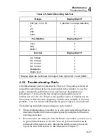
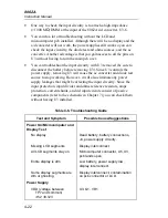
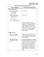

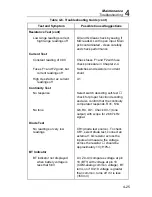

Maintenance
Troubleshooting
4
4-27
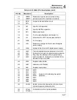
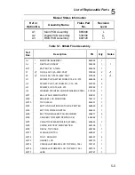
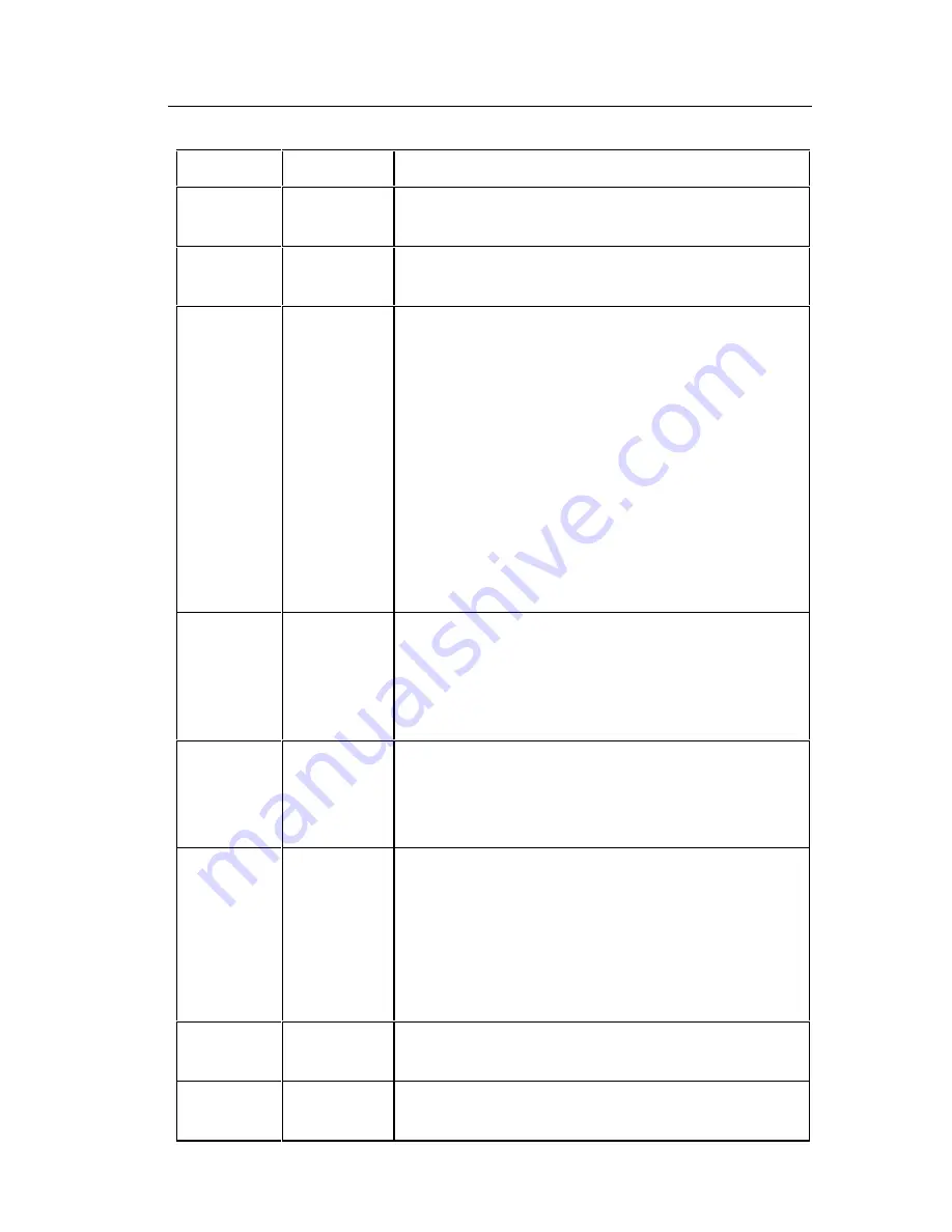
Table 4-8. U3 (MAC) Pin Descriptions (cont)
Pin No.
Mnemonic
Description
12
13
OREF-
OREF+
Reference input to a/d converter during
autozero period for resistance functions.
14
15
BFH
BFL
Output of the a/d buffer circuit.
16
17
18
19
20
21
22
23
AZ
INT
BTI
VIA
CV
VDD
VID
VDG
Input for AZ capacitor.
Input for INTEG capacitor.
Battery test input.
+5.2V supply feedback (nominally 1V)
Gate drive for JFET. Series pass element
+5.2V supply.
Reference voltage for the U3 and U5 digital
power supply.
Output of the U3 and U5 digital power supply.
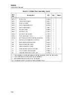
24
25
26
27
AD0
AD1
AD2
AD3
Four-bit parallel data bus between U3 and U5.
During the first part of a data transfer operation
they carry the address of the register being
read or written to. During the remainder of the
operation they carry data.
28
29
30
WR/
ALE/
RD/
Register write strobe.
Address Latch Enable.
Register read strobe.
31
32
33
34
35
36
37
IN10
IN11
IN12
IN13
IN20
IN21
IN22
SW5
SW6
SW7
Inputs to U5 indicating the switch
SW8
positions.
SW1
SW2
SW3
38
CLKO
40 kHz clock which drives the U5 clock input
(crystal frequency divided by 80).
39
40
XTALI
XTALO
Connections to the crystal oscillator.
Summary of Contents for 8062A
Page 4: ......
Page 8: ...8062A Instruction Manual iv...
Page 10: ...8062A Instruction Manual vi...
Page 14: ...8062A Instruction Manual 1 2...
Page 24: ...8062A Instruction Manual 2 2...
Page 50: ...8062A Instruction Manual 2 28...
Page 52: ...8062A Instruction Manual 3 2...
Page 62: ...8062A Instruction Manual 3 12...
Page 64: ...8062A Instruction Manual 4 2...
Page 90: ...8062A Instruction Manual 4 28...
Page 92: ...8062A Instruction Manual 5 2...
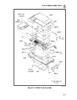
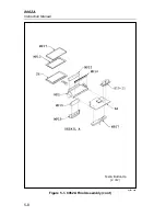
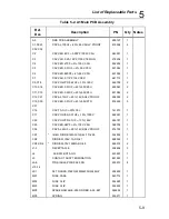
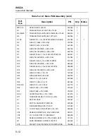
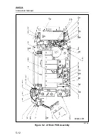
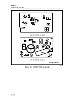
Page 102: ...8062A Instruction Manual 5 12 8062A 4031 iv39c eps Figure 5 2 A1 Main PCB Assembly...
Page 106: ...8062A Instruction Manual 6 2...
Page 108: ...8062A Instruction Manual 6 4 dy55c eps Figure 6 1 Accessories...
Page 118: ...8062A Instruction Manual 7 2...
Page 122: ...8062A Instruction Manual 7 6...
Page 123: ...8062A Instruction Manual 7 7 8062A 1201 iu46c eps Figure 7 5 A1 Main PCB Schmatic Diagram...
Page 124: ...8062A Instruction Manual 7 8 8060A 1003 iu61f eps Figure 7 6 A3 RMS PCB Schmatic Diagram...


