


Safety Information
This meter has been designed and tested in accordance with IEC Publication
348. To ensure that the meter is used safely, follow all safety and operating
instructions in this manual. If the meter is not used as described in this man-
ual, the safety features of the meter might be impaired.
•
Do not use the meter if the meter or test leads look damaged, or if you
suspect that the meter is not operating properly.
•
Turn off power to the circuit under test before cutting, unsoldering, or
breaking the circuit. Small amounts of current can be dangerous.
•
Do not apply more than 500V rms between a terminal and earth ground.
•
Use caution when working above 60V dc or 30V ac rms. Such voltages
pose a shock hazard.
•
When using the probes, keep your fingers behind the finger guards on
the probes.
•
Disconnect the live test lead before disconnecting the common test lead.
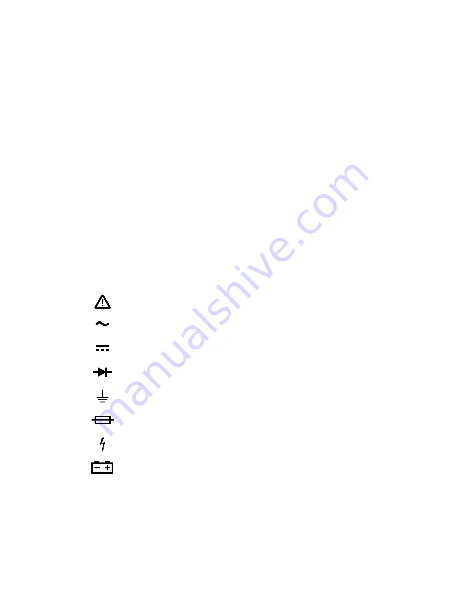
Symbols
The following international symbols are used in this manual:
Important Safety Information in Manual
AC
DC
Diode Test
Ground
Fuse
Indicates Terminals At Which Dangerous Voltages May Exist
Battery
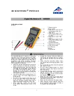
Summary of Contents for 8062A
Page 4: ......
Page 8: ...8062A Instruction Manual iv...
Page 10: ...8062A Instruction Manual vi...
Page 14: ...8062A Instruction Manual 1 2...
Page 24: ...8062A Instruction Manual 2 2...
Page 50: ...8062A Instruction Manual 2 28...
Page 52: ...8062A Instruction Manual 3 2...
Page 62: ...8062A Instruction Manual 3 12...
Page 64: ...8062A Instruction Manual 4 2...
Page 90: ...8062A Instruction Manual 4 28...
Page 92: ...8062A Instruction Manual 5 2...
Page 102: ...8062A Instruction Manual 5 12 8062A 4031 iv39c eps Figure 5 2 A1 Main PCB Assembly...
Page 106: ...8062A Instruction Manual 6 2...
Page 108: ...8062A Instruction Manual 6 4 dy55c eps Figure 6 1 Accessories...
Page 118: ...8062A Instruction Manual 7 2...
Page 122: ...8062A Instruction Manual 7 6...
Page 123: ...8062A Instruction Manual 7 7 8062A 1201 iu46c eps Figure 7 5 A1 Main PCB Schmatic Diagram...
Page 124: ...8062A Instruction Manual 7 8 8060A 1003 iu61f eps Figure 7 6 A3 RMS PCB Schmatic Diagram...