


AT32WB415
Series Reference Manual
2022.04.13
Page 115
Ver 2.00
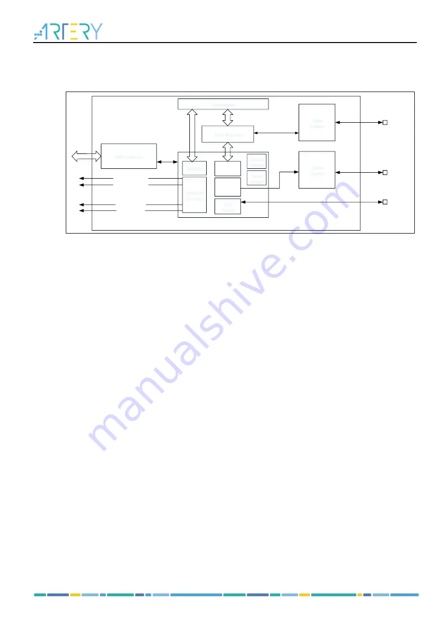
11.4 I
2
C interface
Figure 11-2 shows the block diagram of I
2
C function
Figure 11-2 I2C function block diagram
APB Interface
Interrupt
Generation
I2C_DMA_req_tx
I2C_DMA_req_rx
Register
Alert
control
Data
Register
Data
Control
Clock
Control
I2C_Event_intr
I2C_Error_intr
SDA
SCL
Clock
Control
Register
Shift Register
SMBALERT
Control
register
Status
register
Comparator
OADDR
I2C
1. I
2
C clock
I
2
C is clocked by either APB1 or APB2. The I
2
C clock division is achieved by setting the CLKFREQ[7:
0] in the I2C_CTRL2 register. The minimum clock frequency varies from one mode to another, that
is, at least 2 MHz in standard mode, but 4 MHz in fast mode.
2. Operating mode
I
2
C bus interface can operate both in master mode and slave mode. Switching from master mode to
slave mode, vice versa, is supported as well. By default, the interface operates in slave mode. When
GENSTART=1 is set (Start condition is activated), the I
2
C bus interface switches from slave mode to
master mode, and returns to slave mode automatcially at the end of data transfer (Stop condition is
triggered).
Master transmitter
Master receiver
Slave transmitter
Slave receiver
3. Communication process
Master mode communication:
1.
Start condition generation
2.
Address transmission
3.
Data Tx or Rx
4.
Stop condition generation
5.
End of communication
Slave mode communication:
1.
Wait until the address is matched.
2.
Data Tx or Rx
3.
Wait for the generation of Stop condition
4.
End of communication
4. Address control
Both master and slave support 7-bit and 10-bit addressing modes.
Slave address mode:
In 7-bit mode
―
ADDR2EN=0 stands for a single address mode: only matches OADDR1
―
DUALEN=1
stands for dual address mode: matches OADDR1 and OADDR2


