


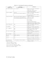


T
able
B-1.
Signal
Name
(continued)
Mnemonic
Description
Pin
Assignment
GND
Ground
(continued)
,J4-C8,J4-C9,J5-A10,J5-A11,J5-A12,J5-A1,J5-A22
,J5-A23,J5-A24,J5-A26,J5-A27,J5-A28,J5-A30,J5-A32
,J5-A8,J5-B10,J5-B11,J5-B12,J5-B1,J5-B23,J5-B24
,J5-B25,J5-B26,J5-B28,J5-B29,J5-B30,J5-B31,J5-B32
,J5-B8,J5-C10,J5-C11,J5-C1,J5-C20,J5-C21,J5-C23
,J5-C24,J5-C25,J5-C26,J5-C27,J5-C28,J5-C29,J5-C8
,J6-A19,J6-A1,J6-A27,J6-A29,J6-A30,J6-A32,J6-A8
,J6-A9,J6-B12,J6-B1,J6-B28,J6-B29,J6-B31,J6-B8
,J6-B9,J6-C19,J6-C1,J6-C28,J6-C29,J6-C30,J6-C8
,J6-C9,J7-2,J8-A10,J8-A11,J8-A12,J8-A1,J8-A22
,J8-A23,J8-A24,J8-A26,J8-A27,J8-A28,J8-A29,J8-A30
,J8-A31,J8-A32,J8-A8,J8-A9,J8-B10,J8-B11,J8-B12
,J8-B1,J8-B23,J8-B24,J8-B25,J8-B26,J8-B28,J8-B29
,J8-B30,J8-B31,J8-B32,J8-B8,J8-B9,J8-C11,J8-C19
,J8-C1,J8-C20,J8-C21,J8-C23,J8-C24,J8-C25,J8-C26
,J8-C27,J8-C28,J8-C29,J8-C8,J8-C9
A1
A
ddress
Bus
(Bit
1)
J1-34,J2-B20,J3-B13,J4-B13,J5-B13,J6-B13,J8-B13
A2
A
ddress
Bus
(Bit
2)
J1-84,J2-C20,J3-A13,J4-A13,J5-A13,J6-A13,J8-A13
AD
CLOCK
A/D
Sync
Clock
J1-10,J6-A20
AD
D
A
T
A
A/D
Serial
Data
J1-61,J6-A21
A
TT
IN
10
Input
Attenuator
10
dB
Select
J2-A2,J20-1
A
TT
IN
20
Input
Attenuator
20
dB
Select
J2-B2,J20-2
A
TT
IN
30
Input
Attenuator
30
dB
Select
J2-C2,J20-3
A
TT
OUT
10
Output
Attenuator
10
dB
Select
J2-A3,J20-4
A
TT
OUT
20
Output
Attenuator
20
dB
Select
J2-B3,J20-5
A
TT
OUT
30
Output
Attenuator
30
dB
Select
J2-C3,J20-6
A
UTOZERO
A
uto
Zero
Control
J4-A19,J6-B26
CH
A
A
Input
Select
J14-4,J6-C23
CH
B
B
Input
Select
J14-5,J6-C24
CH
R
R
Input
Select
J14-3,J6-C22
CS
A2
A2
Register
Select
J1-37,J2-B21
CS
A2S
A2
Reg.
Select
for
Service
Modes
J1-87,J2-C21
CS
A3
A3
Register
Select
J1-38,J3-B9
CS
A3S
A3
Reg.
Select
for
Service
Modes
J1-88,J3-A9
CS
A4
A4
Register
Select
J1-39,J4-B9
CS
A4S
A4
Reg.
Select
for
Service
Modes
J1-89,J4-A9
CS
A5S
A5
Reg.
Select
for
Service
Modes
J1-90,J5-A9
CS
A6S
A6
Reg.
Select
for
Service
Modes
J1-91,J6-A10
CS
A
UTOZERO
A
uto
Zero
Select
J1-5,J6-A24
CS
BW
Bandwidth
Register
Select
J1-92,J6-A11
CS
CHF
CHNG
Channel/Frequency
Change
J1-55,J6-B24
CS
D
A
C
D
A
C
Select
J1-42,J6-B10
CS
DISCONT
Discontinue
Sense
J1-6,J6-B23
CS
ENHANCE
Enhance
Board
Register
Select
J1-94,J8-C10
A20
Motherboard
Pin
Assignment
B-5
Summary of Contents for Agilent 4396B
Page 10: ......
Page 32: ......
Page 43: ...Figure 2 7 CAL OUT Level Adjustment Location Adjustments and Correction Constants 2 11 ...
Page 46: ...Figure 2 10 Comb Generator Output 2 14 Adjustments and Correction Constants ...
Page 62: ...Figure 2 26 Final Gain Adjustment Location 2 30 Adjustments and Correction Constants ...
Page 76: ...Figure 3 1 Troubleshooting Organization 3 2 T roubleshooting ...
Page 84: ......
Page 90: ...Figure 5 1 Power Supply Lines Simpli ed Block Diagram 5 2 Power Supply T roubleshooting ...
Page 107: ...Figure 5 12 Power Supply Block Diagram 1 Power Supply T roubleshooting 5 19 ...
Page 108: ...Figure 5 13 Power Supply Block Diagram 2 5 20 Power Supply T roubleshooting ...
Page 109: ...Figure 5 14 Power Supply Block Diagram 3 Power Supply T roubleshooting 5 21 ...
Page 110: ......
Page 112: ...Figure 6 1 Digital Control Group Simpli ed Block Diagram 6 2 Digital Control T roubleshooting ...
Page 124: ......
Page 126: ...Figure 7 1 Source Group Block Diagram 7 2 Source Group T roubleshooting ...
Page 160: ...Figure 8 1 Receiver Group Simpli ed Block Diagram 8 2 Receiver Group T roubleshooting ...
Page 168: ......
Page 184: ...Figure 10 6 External Test Setup 1 Figure 10 7 External Test Setup 2 10 10 Service Key Menus ...
Page 185: ...Figure 10 8 External Test Setup 3 Figure 10 9 External Test Setup 4 Service Key Menus 10 11 ...
Page 226: ...Figure 11 3 Power Supply Functional Group Simpli ed Block Diagram 11 6 Theory of Operation ...
Page 231: ...Figure 11 5 Digital Control Group Simpli ed Block Diagram Theory of Operation 11 11 ...
Page 235: ...Figure 11 6 Source Simpli ed Block Diagram Theory of Operation 11 15 ...
Page 244: ...Figure 11 7 Receiver Simpli ed Block Diagram 11 24 Theory of Operation ...
Page 249: ...Figure IDC5S11001 here Figure 11 8 4396B Source Group Block Diagram Theory of Operation 11 29 ...
Page 254: ...Figure 12 1 Top View Major Assemblies 12 4 Replaceable Parts ...
Page 290: ...Figure 12 36 Main Frame Assembly Parts 17 19 12 40 Replaceable Parts ...
Page 294: ......
Page 308: ......
Page 311: ...Figure C 1 Power Cable Supplied Power Requirement C 3 ...
Page 312: ......
Page 324: ......


