


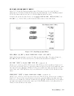


Figure
10-15.
DET
OUT
,
L
VL
CONT
,
and
D
A
C
OUT
Typical
Traces
16:
L
VL
CONT
(Level
V
ernier
Control
V
oltage)
This
node
is
located
in
the
ALC
circuit
on
the
A3A1
ALC
and
detects
the
level
vernier
control
voltage
.
See
Figure
11-6.
The
typical
trace
for
the
following
keystrokes'
setting
is
displayed
as
the
L
VL
CONT
trace
in
Figure
10-15.
4
Meas
5 ,
NNNNNNNNNNNNNNNNNNNNNNNNNNNNNNNNNNNNNNNNN
ANALYZER
TYPE
,
NNNNNNNNNNNNNNNNNNNNNNNNNNNNNNNNNNNNNNNNNNNNNNNNNN
NETWORK
ANALYZER
,
4
Preset
5 ,
4
Sw
eep
5 ,
NNNNNNNNNNNNNNNNNNNNNNNNNNNNNNNNNNNNNNNNNNNNNNNNNN
NUMBER
of
POINTS
,
4
7
5 ,
4
x1
5 ,
4
Sw
eep
5 ,
NNNNNNNNNNNNNNNNNNNNNNNNNNNNNNNNNNNNNNNNNNNNNNN
SWEEP
TYPE
MENU
,
NNNNNNNNNNNNNNNNNNNNNNNNNNNNNNNNNNN
POWER
SWEEP
,
4
Start
5 ,
4
-
5 ,
4
2
5 ,
4
0
5 ,
4
x1
5 ,
4
Stop
5 ,
4
1
5 ,
4
0
5 ,
4
x1
5
T
o
observe
the
trace
,
perform
the
steps
in
the
Bus
Measurement
Procedure
.
At
step
2
in
the
procedure
,
press
the
keys
listed
above
.
17:
D
A
C
OUT
(Level
D
A
C
Output
V
oltage)
This
node
is
located
in
the
ALC
circuit
on
the
A3A1
ALC
and
detects
the
level
D
A
C
output
voltage
.
See
Figure
10-15.
The
typical
trace
for
the
following
keystrokes'
setting
is
displayed
as
the
D
A
C
OUT
trace
in
Figure
10-15.
4
Meas
5 ,
NNNNNNNNNNNNNNNNNNNNNNNNNNNNNNNNNNNNNNNNN
ANALYZER
TYPE
,
NNNNNNNNNNNNNNNNNNNNNNNNNNNNNNNNNNNNNNNNNNNNNNNNNN
NETWORK
ANALYZER
,
4
Preset
5 ,
4
Sw
eep
5 ,
NNNNNNNNNNNNNNNNNNNNNNNNNNNNNNNNNNNNNNNNNNNNNNNNNN
NUMBER
of
POINTS
,
4
7
5 ,
4
x1
5 ,
4
Sw
eep
5 ,
NNNNNNNNNNNNNNNNNNNNNNNNNNNNNNNNNNNNNNNNNNNNNNN
SWEEP
TYPE
MENU
,
NNNNNNNNNNNNNNNNNNNNNNNNNNNNNNNNNNN
POWER
SWEEP
,
4
Start
5 ,
4
-
5 ,
4
2
5 ,
4
0
5 ,
4
x1
5 ,
4
Stop
5 ,
4
1
5 ,
4
0
5 ,
4
x1
5
T
o
observe
this
trace
,
perform
the
steps
in
the
Bus
Measurement
Procedure
.
At
step
2
in
the
procedure
,
press
the
keys
listed
above
.
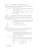
18:
1ST
LO
VTUNE
(First
Local
Oscillator
V
CO
Turning
V
oltage)
This
node
is
located
in
the
1st
local
oscillator
on
the
A4A1
1st
LO
and
detects
the
2.05858
GHz
to
3.85858
GHz
V
CO
tuning
voltage
.
See
Figure
11-6.
The
typical
trace
for
the
following
keystrokes'
setting
is
displayed
in
Figure
10-16.
The
displayed
trace
is
typically
straight.
The
typical
marker
value
is
within
02.3
U
to
01.2
U
at
a
frequency
of
100
kHz
and
within
+0.1
U
to
+1.9
U
at
a
frequency
1.8
GHz.
10-26
Service
K
ey
Menus
Summary of Contents for Agilent 4396B
Page 10: ......
Page 32: ......
Page 43: ...Figure 2 7 CAL OUT Level Adjustment Location Adjustments and Correction Constants 2 11 ...
Page 46: ...Figure 2 10 Comb Generator Output 2 14 Adjustments and Correction Constants ...
Page 62: ...Figure 2 26 Final Gain Adjustment Location 2 30 Adjustments and Correction Constants ...
Page 76: ...Figure 3 1 Troubleshooting Organization 3 2 T roubleshooting ...
Page 84: ......
Page 90: ...Figure 5 1 Power Supply Lines Simpli ed Block Diagram 5 2 Power Supply T roubleshooting ...
Page 107: ...Figure 5 12 Power Supply Block Diagram 1 Power Supply T roubleshooting 5 19 ...
Page 108: ...Figure 5 13 Power Supply Block Diagram 2 5 20 Power Supply T roubleshooting ...
Page 109: ...Figure 5 14 Power Supply Block Diagram 3 Power Supply T roubleshooting 5 21 ...
Page 110: ......
Page 112: ...Figure 6 1 Digital Control Group Simpli ed Block Diagram 6 2 Digital Control T roubleshooting ...
Page 124: ......
Page 126: ...Figure 7 1 Source Group Block Diagram 7 2 Source Group T roubleshooting ...
Page 160: ...Figure 8 1 Receiver Group Simpli ed Block Diagram 8 2 Receiver Group T roubleshooting ...
Page 168: ......
Page 184: ...Figure 10 6 External Test Setup 1 Figure 10 7 External Test Setup 2 10 10 Service Key Menus ...
Page 185: ...Figure 10 8 External Test Setup 3 Figure 10 9 External Test Setup 4 Service Key Menus 10 11 ...
Page 226: ...Figure 11 3 Power Supply Functional Group Simpli ed Block Diagram 11 6 Theory of Operation ...
Page 231: ...Figure 11 5 Digital Control Group Simpli ed Block Diagram Theory of Operation 11 11 ...
Page 235: ...Figure 11 6 Source Simpli ed Block Diagram Theory of Operation 11 15 ...
Page 244: ...Figure 11 7 Receiver Simpli ed Block Diagram 11 24 Theory of Operation ...
Page 249: ...Figure IDC5S11001 here Figure 11 8 4396B Source Group Block Diagram Theory of Operation 11 29 ...
Page 254: ...Figure 12 1 Top View Major Assemblies 12 4 Replaceable Parts ...
Page 290: ...Figure 12 36 Main Frame Assembly Parts 17 19 12 40 Replaceable Parts ...
Page 294: ......
Page 308: ......
Page 311: ...Figure C 1 Power Cable Supplied Power Requirement C 3 ...
Page 312: ......
Page 324: ......


