


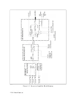


The
oscillator
contains
an
85.68
MHz
V
CO
,
a
phase
detector
,
a
1/2
divider
,
a
mixer
,
and
a
1/71
divider
.
See
Figure
11-6.
The
V
CO
frequency
(F
vco
)
is
divided
by
2
and
mixed
with
the
40
MHz
reference
frequency
in
the
mixer
.
The
mixer
then
produces
a
shifted
frequency
(F
vco
/2
0
40
MHz).
The
mixer
output
is
divided
by
71
and
then
compared
with
the
40
kHz
reference
signal
in
the
phase
detector
.
Phase
locking
imposes
the
condition
of
40
kHz
=
(F
vco
/2
0
40
MHz)/71.
Therefore
,
the
output
frequency
(F
vco
)
is
locked
to
85.68
MHz
(=
(40
kHz
x
71
+
40
MHz)
x
2).
ALC
The
ALC
controls
the
level
of
the
21.42
MHz
CW
signal
from
the
source
OSC.
The
signal
is
routed
to
the
RF
OUT
connector
through
the
A3A2
2nd
LO
,
the
A3A3
source
,
and
the
A7
Output
Attenuator
.
The
A3A3
output
level
is
detected
and
loops
back
to
the
ALC
for
automatic
leveling
control.
The
ALC
consists
of
a
level
D
A
C,
an
error
detector
,
an
integrator
,
a
Gain
ALC,
and
a
level
vernier
.
See
Figure
11-6.
In
addition,
a
switch
that
follows
the
level
vernier
is
used
to
turn
the
RF
OUT
signal
on
and
o.
The
loop-backed
A3A3
output
level
is
compared
with
the
level
D
A
C
output
in
the
error
detector
.
The
error
detector
produces
a
DC
voltage
proportional
to
the
error
between
the
A3A3
output
level
and
the
level
D
A
C
output.
The
error
detector
output
controls
the
21.42
MHz
signal
level
through
the
integrator
and
the
level
vernier
.
ALC
loop
locking
imposes
the
condition
of
Level
D
A
C
Output
=
A3A3
Output
Level.
Therefore
,
the
A3A3
output
level
is
determined
by
the
level
D
A
C
setting.
The
A3A3
output
level
for
each
level
D
A
C
setting
is
predened
by
performing
the
RF
OUT
Level
Correction
Constants.
The
predened
data
is
stored
in
the
EEPROM
of
the
A1
CPU
.
The
Gain
ALC
is
a
variable
amplier
from
0
dB
to
6
dB
.
It
is
used
to
shorten
the
time
required
for
the
ALC
loop
to
be
locked
after
the
frequency
is
changed.
It
does
this
by
compensating
the
frequency
response
of
the
source
amplier's
gain
in
the
A3A3
source
.
Therefore
,
the
Gain
ALC
setting
depends
on
the
RF
signal
frequency
.
The
Gain
ALC
settings
are
predened
over
the
entire
frequency
range
by
performing
the
RF
OUT
Level
Correction
Constants.
The
predened
setting
data
is
stored
in
the
EEPROM
of
the
A1
CPU
.
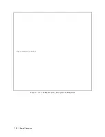
A3A2
2nd
LO
The
A3A2
2nd
LO
generates
the
second
local
oscillator
signal
(a
2.08
GHz
CW
signal)
and
converts
the
21.42
MHz
signal
from
the
A3A1
ALC
to
a
2.05858
GHz
IF
signal
by
mixing
the
21.42
MHz
and
the
second
local
oscillator
signal.
The
2.05858
GHz
IF
signal
is
supplied
to
the
A3A3
source
and
then
converter
to
a
swept
RF
signal.
The
second
local
oscillator
signal
is
supplied
to
the
A4A2
receiver
RF
.
The
A3A1
ALC
consists
of
the
following
circuits:
2nd
LO
Source
First
Mixer
2nd
Local
OSC
Circuit
The
2nd
Local
oscillator
circuit
is
a
phase
locked
oscillator
.
The
output
signal
is
phase
locked
to
the
520
MHz
frequency
from
the
A5
synthesizer
.
The
oscillator
generates
a
2.08
GHz
signal.
The
signal
is
supplied
to
the
source
rst
mixer
and
the
A4A1
receiver
RF
.
The
oscillator
contains
a
1.04
GHz
V
CO
,
a
phase
detector
,
and
a
1/2
divider
.
See
Figure
11-6 .
The
V
CO
frequency
(F
vco
)
is
divided
by
2
and
then
compared
with
the
520
MHz
reference
signal
in
the
phase
detector
.
Phase
locking
imposes
the
condition
of
520
MHz
=
F
vco
/2.
Therefore
,
the
output
frequency
(F
vco
)
is
locked
to
1.04
GHz
(=
520
MHz
x
2).
Then
the
signal
frequency
is
converted
to
2.08
GHz
by
the
doubler
.
11-20
Theory
of
Operation
Summary of Contents for Agilent 4396B
Page 10: ......
Page 32: ......
Page 43: ...Figure 2 7 CAL OUT Level Adjustment Location Adjustments and Correction Constants 2 11 ...
Page 46: ...Figure 2 10 Comb Generator Output 2 14 Adjustments and Correction Constants ...
Page 62: ...Figure 2 26 Final Gain Adjustment Location 2 30 Adjustments and Correction Constants ...
Page 76: ...Figure 3 1 Troubleshooting Organization 3 2 T roubleshooting ...
Page 84: ......
Page 90: ...Figure 5 1 Power Supply Lines Simpli ed Block Diagram 5 2 Power Supply T roubleshooting ...
Page 107: ...Figure 5 12 Power Supply Block Diagram 1 Power Supply T roubleshooting 5 19 ...
Page 108: ...Figure 5 13 Power Supply Block Diagram 2 5 20 Power Supply T roubleshooting ...
Page 109: ...Figure 5 14 Power Supply Block Diagram 3 Power Supply T roubleshooting 5 21 ...
Page 110: ......
Page 112: ...Figure 6 1 Digital Control Group Simpli ed Block Diagram 6 2 Digital Control T roubleshooting ...
Page 124: ......
Page 126: ...Figure 7 1 Source Group Block Diagram 7 2 Source Group T roubleshooting ...
Page 160: ...Figure 8 1 Receiver Group Simpli ed Block Diagram 8 2 Receiver Group T roubleshooting ...
Page 168: ......
Page 184: ...Figure 10 6 External Test Setup 1 Figure 10 7 External Test Setup 2 10 10 Service Key Menus ...
Page 185: ...Figure 10 8 External Test Setup 3 Figure 10 9 External Test Setup 4 Service Key Menus 10 11 ...
Page 226: ...Figure 11 3 Power Supply Functional Group Simpli ed Block Diagram 11 6 Theory of Operation ...
Page 231: ...Figure 11 5 Digital Control Group Simpli ed Block Diagram Theory of Operation 11 11 ...
Page 235: ...Figure 11 6 Source Simpli ed Block Diagram Theory of Operation 11 15 ...
Page 244: ...Figure 11 7 Receiver Simpli ed Block Diagram 11 24 Theory of Operation ...
Page 249: ...Figure IDC5S11001 here Figure 11 8 4396B Source Group Block Diagram Theory of Operation 11 29 ...
Page 254: ...Figure 12 1 Top View Major Assemblies 12 4 Replaceable Parts ...
Page 290: ...Figure 12 36 Main Frame Assembly Parts 17 19 12 40 Replaceable Parts ...
Page 294: ......
Page 308: ......
Page 311: ...Figure C 1 Power Cable Supplied Power Requirement C 3 ...
Page 312: ......
Page 324: ......


