


Bus
Measurement
V
alues
The
bus
measurement
value
is
displayed
with
a
unit
\U
."
The
DC
bus
measurement's
\1
U"
is
equivalent
to
\1
V
."
The
displayed
value
in
the
DC
bus
measurement
does
not
corresponding
to
the
measured
voltage
because
the
voltage
detected
at
the
DC
bus
node
is
scaled
appropriately
and
measured.
The
scaling
factor
depends
on
each
DC
node
.
F
or
example
,
the
scaling
factor
at
the
DC
bus
node
1
of
+5
V
(A
UX)
is
approximately
0.405.
Therefore
the
displayed
value
is
nominally
2.025
U
(5
U
x
0.405).
A
typical
value
for
each
DC
bus
node
measurement
is
provided
in
the
DC
Bus
Node
Descriptions.
The
frequency
bus
measurement's
\1
U"
is
equivalent
to
\1
MHz."
F
or
example
,
a
measured
value
of
1
kHz
is
displayed
as
1
mU
.
A
typical
value
for
each
frequency
bus
measurement
is
provided
in
the
Frequency
Bus
Node
Descriptions.
The
DC
bus
measurement
values
are
displayed
using
real
format.
The
frequency
bus
measurement
values
are
displayed
using
imaginary
format.
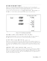
When
a
DC
or
Frequency
bus
node
is
measured,
the
Re
or
Im
notation
appears
on
the
display
and
indicates
the
used
format.
When
both
a
DC
bus
node
and
a
frequency
bus
node
are
measured
simultaneously
,
the
DC
bus
versus
frequency
bus
measurement
values
are
displayed
using
a
polar
chart
format.
This
is
helpful
to
observe
the
relationship
between
the
V
CO
tuning
voltage
and
the
V
CO
output
frequency
of
the
fractional
N
oscillator
.
DC
Bus
Node
Descriptions
The
following
paragraphs
describe
the
26
DC
bus
nodes
.
They
are
listed
in
numerical
order
.
0:
NONE
The
DC
bus
is
o.
This
is
the
default
setting.
1:
+5
V
(A
UX)
(2.025
U)
This
node
is
located
on
the
A2
post-regulator
and
detects
the
voltage
of
the
+5
V
(A
UX)
power
supplied
to
the
A2
post-
regulator
.
See
Figure
5-1.
T
o
observe
this
node
,
perform
the
steps
in
the
Bus
Measurement
Procedure
.
When
this
node
is
selected,
the
trace
is
typically
at
at
approximately
+2.025
U
(610%).
2:
015
V
(01.92
U)
This
node
is
located
on
the
A2
post-regulator
and
detects
the
voltage
of
the
+5
V
(A
UX)
power
supplied
to
the
analog
boards
.
See
Figure
5-1.
T
o
observe
this
node
,
perform
the
steps
in
the
Bus
Measurement
Procedure
.
When
this
node
is
selected,
the
trace
is
typically
at
at
approximately
01.92
U
(610%).
3:
012.6
V
(02.124
U)
This
node
is
located
on
the
A2
post-regulator
and
detects
the
voltage
of
the
012.6
V
power
supplied
to
the
probe
power
connectors
on
the
front
panel.
See
Figure
5-1.
T
o
observe
this
node
,
perform
the
steps
in
the
Bus
Measurement
Procedure
.
When
this
node
is
selected,
the
trace
is
typically
at
at
approximately
02.124
U
(610%).
Service
K
ey
Menus
10-23
Summary of Contents for Agilent 4396B
Page 10: ......
Page 32: ......
Page 43: ...Figure 2 7 CAL OUT Level Adjustment Location Adjustments and Correction Constants 2 11 ...
Page 46: ...Figure 2 10 Comb Generator Output 2 14 Adjustments and Correction Constants ...
Page 62: ...Figure 2 26 Final Gain Adjustment Location 2 30 Adjustments and Correction Constants ...
Page 76: ...Figure 3 1 Troubleshooting Organization 3 2 T roubleshooting ...
Page 84: ......
Page 90: ...Figure 5 1 Power Supply Lines Simpli ed Block Diagram 5 2 Power Supply T roubleshooting ...
Page 107: ...Figure 5 12 Power Supply Block Diagram 1 Power Supply T roubleshooting 5 19 ...
Page 108: ...Figure 5 13 Power Supply Block Diagram 2 5 20 Power Supply T roubleshooting ...
Page 109: ...Figure 5 14 Power Supply Block Diagram 3 Power Supply T roubleshooting 5 21 ...
Page 110: ......
Page 112: ...Figure 6 1 Digital Control Group Simpli ed Block Diagram 6 2 Digital Control T roubleshooting ...
Page 124: ......
Page 126: ...Figure 7 1 Source Group Block Diagram 7 2 Source Group T roubleshooting ...
Page 160: ...Figure 8 1 Receiver Group Simpli ed Block Diagram 8 2 Receiver Group T roubleshooting ...
Page 168: ......
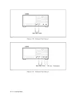
Page 184: ...Figure 10 6 External Test Setup 1 Figure 10 7 External Test Setup 2 10 10 Service Key Menus ...
Page 185: ...Figure 10 8 External Test Setup 3 Figure 10 9 External Test Setup 4 Service Key Menus 10 11 ...
Page 226: ...Figure 11 3 Power Supply Functional Group Simpli ed Block Diagram 11 6 Theory of Operation ...
Page 231: ...Figure 11 5 Digital Control Group Simpli ed Block Diagram Theory of Operation 11 11 ...
Page 235: ...Figure 11 6 Source Simpli ed Block Diagram Theory of Operation 11 15 ...
Page 244: ...Figure 11 7 Receiver Simpli ed Block Diagram 11 24 Theory of Operation ...
Page 249: ...Figure IDC5S11001 here Figure 11 8 4396B Source Group Block Diagram Theory of Operation 11 29 ...
Page 254: ...Figure 12 1 Top View Major Assemblies 12 4 Replaceable Parts ...
Page 290: ...Figure 12 36 Main Frame Assembly Parts 17 19 12 40 Replaceable Parts ...
Page 294: ......
Page 308: ......
Page 311: ...Figure C 1 Power Cable Supplied Power Requirement C 3 ...
Page 312: ......
Page 324: ......


