


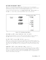


26:
GND
(Ground)
This
node
is
located
on
the
A2
post-regulator
and
detects
the
ground
voltage
.
See
Figure
5-1.
T
o
observe
this
node
,
perform
the
steps
in
the
Bus
Measurement
Procedure.
When
this
node
is
selected,
the
trace
is
typically
at
and
within
00.1
to
+0.1.
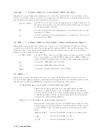
Frequency
Bus
Node
Descriptions
The
following
paragraphs
describe
the
6
frequency
bus
nodes
.
They
are
listed
in
numerical
order
.
0:
OFF
The
frequency
bus
is
o.
This
is
the
default
setting.
1:
SOURCE
OSC
(Source
Oscillator)
This
node
is
located
in
the
source
oscillator
on
the
A3A1
ALC
and
measures
the
loop
back
frequency
of
40
kHz
from
the
85.68
MHz
V
CO
.
See
Figure
11-6 .
The
typical
trace
for
the
following
keystrokes'
setting
is
at
and
within
+39.992
mU
to
+40.008
mU
.
4
Meas
5 ,
NNNNNNNNNNNNNNNNNNNNNNNNNNNNNNNNNNNNNNNNN
ANALYZER
TYPE
,
NNNNNNNNNNNNNNNNNNNNNNNNNNNNNNNNNNNNNNNNNNNNNNNNNN
NETWORK
ANALYZER
,
4
Preset
5 ,
4
Sw
eep
5 ,
NNNNNNNNNNNNNNNNNNNNNNNNNNNNNNNNNNNNNNNNNNNNNNNNNN
NUMBER
OF
POINTS
,
4
2
5 ,
4
x1
5
T
o
observe
this
node
,
perform
the
steps
in
the
Bus
Measurement
Procedure
.
At
step
2
in
the
procedure
,
press
the
keys
listed
above
.
2:
DIVIDER
OUT
(Divider
Output)
This
node
is
located
in
the
divider
on
the
A3A1
ALC
and
measures
the
1/200
divider
output
frequency
40
kHz.
See
Figure
11-6 .
The
typical
trace
is
at
and
within
+39.992
mU
to
+40.008
mU
.
T
o
observe
this
node
,
perform
the
steps
in
the
Bus
Measurement
Procedure
.
At
step
2
in
the
procedure
,
press
the
keys
listed
below
to
make
a
fast
sweep
.
4
Meas
5 ,
NNNNNNNNNNNNNNNNNNNNNNNNNNNNNNNNNNNNNNNNN
ANALYZER
TYPE
,
NNNNNNNNNNNNNNNNNNNNNNNNNNNNNNNNNNNNNNNNNNNNNNNNNN
NETWORK
ANALYZER
,
4
Preset
5 ,
4
Sw
eep
5 ,
NNNNNNNNNNNNNNNNNNNNNNNNNNNNNNNNNNNNNNNNNNNNNNNNNN
NUMBER
OF
POINTS
,
4
1
5 ,
4
0
5 ,
4
x1
5
3:
STEP
OSC
(Step
Oscillator)
This
node
is
located
in
the
step
oscillator
on
the
A5
synthesizer
and
measures
the
step
oscillator
frequency
through
the
1/256
divider
.
See
Figure
11-6.
The
typical
trace
is
at
and
the
trace
value
depends
on
the
measurement
settings
(center
and
span
settings).
The
typical
values
for
several
settings
are
provided
in
T
able
7-1
STEP
OSC
Frequency
in
chapter
7.
4:
FN
OSC
(Fractional
N
Oscillator)
This
node
is
located
in
the
fractional
N
oscillator
on
the
A5
synthesizer
and
measures
the
fractional
N
oscillator
frequency
through
the
1/16
divider
.
See
Figure
11-6.
The
typical
trace
is
at
and
the
trace
value
depends
on
the
measurement
settings
(center
and
span
settings).
The
typical
values
for
several
settings
are
provided
in
the
Check
the
FRA
C
N
OSC
Signal
in
chapter
7.
10-30
Service
K
ey
Menus
Summary of Contents for Agilent 4396B
Page 10: ......
Page 32: ......
Page 43: ...Figure 2 7 CAL OUT Level Adjustment Location Adjustments and Correction Constants 2 11 ...
Page 46: ...Figure 2 10 Comb Generator Output 2 14 Adjustments and Correction Constants ...
Page 62: ...Figure 2 26 Final Gain Adjustment Location 2 30 Adjustments and Correction Constants ...
Page 76: ...Figure 3 1 Troubleshooting Organization 3 2 T roubleshooting ...
Page 84: ......
Page 90: ...Figure 5 1 Power Supply Lines Simpli ed Block Diagram 5 2 Power Supply T roubleshooting ...
Page 107: ...Figure 5 12 Power Supply Block Diagram 1 Power Supply T roubleshooting 5 19 ...
Page 108: ...Figure 5 13 Power Supply Block Diagram 2 5 20 Power Supply T roubleshooting ...
Page 109: ...Figure 5 14 Power Supply Block Diagram 3 Power Supply T roubleshooting 5 21 ...
Page 110: ......
Page 112: ...Figure 6 1 Digital Control Group Simpli ed Block Diagram 6 2 Digital Control T roubleshooting ...
Page 124: ......
Page 126: ...Figure 7 1 Source Group Block Diagram 7 2 Source Group T roubleshooting ...
Page 160: ...Figure 8 1 Receiver Group Simpli ed Block Diagram 8 2 Receiver Group T roubleshooting ...
Page 168: ......
Page 184: ...Figure 10 6 External Test Setup 1 Figure 10 7 External Test Setup 2 10 10 Service Key Menus ...
Page 185: ...Figure 10 8 External Test Setup 3 Figure 10 9 External Test Setup 4 Service Key Menus 10 11 ...
Page 226: ...Figure 11 3 Power Supply Functional Group Simpli ed Block Diagram 11 6 Theory of Operation ...
Page 231: ...Figure 11 5 Digital Control Group Simpli ed Block Diagram Theory of Operation 11 11 ...
Page 235: ...Figure 11 6 Source Simpli ed Block Diagram Theory of Operation 11 15 ...
Page 244: ...Figure 11 7 Receiver Simpli ed Block Diagram 11 24 Theory of Operation ...
Page 249: ...Figure IDC5S11001 here Figure 11 8 4396B Source Group Block Diagram Theory of Operation 11 29 ...
Page 254: ...Figure 12 1 Top View Major Assemblies 12 4 Replaceable Parts ...
Page 290: ...Figure 12 36 Main Frame Assembly Parts 17 19 12 40 Replaceable Parts ...
Page 294: ......
Page 308: ......
Page 311: ...Figure C 1 Power Cable Supplied Power Requirement C 3 ...
Page 312: ......
Page 324: ......


