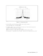


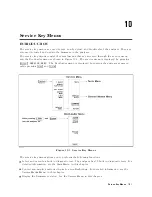


CHECK
SIGNAL
INPUTS
TO
THE
A4A2
RECEIVER
RF
Use
this
procedure
when
the
A4A2
receiver
IF
is
the
most
questionable
assembly
.
A4A2
consists
of
the
NA/SA
Switch,
the
rst
converter
,
and
the
second
converter
.
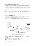
See
the
A4A2
block
in
Figure
8-1 .
P
erform
the
following
procedures
to
verify
the
input
signals
to
A4A2.
If
the
signals
are
good,
replace
A4A2.
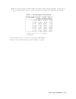
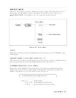
Check
the
Input
Signal
to
A4A2J3
The
input
signal
to
A4A2J3
is
the
rst
local
oscillator
signal
(2.05858
GHz
to
3.85858
GHz)
coming
from
the
A4A1
1st
LO
.
V
erify
the
signal
in
accordance
with
the
Check
the
1st
LO
OSC
Signal
at
A4A1J4.
in
the
Source
Group
Troubleshooting
chapter
.
If
the
input
signal
to
A4A2J3
is
good,
continue
with
the
Check
the
2nd
LO
OSC
Signal
at
A4A2J12.
If
the
input
signal
to
A4A2J3
is
bad,
inspect
the
\F"
semi-
rigid
cable
between
A4A2J3
and
A4A1J4.
If
the
cable
is
good,
continue
with
the
Check
A4A1
1st
LO
Outputs
in
the
Source
Group
Troubleshooting
chapter
.
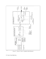
Check
the
Input
Signal
to
A4A2J12
The
input
signal
to
A4A2J12
is
the
2.08
GHz
second
local
oscillator
signal
from
the
A3A2
2nd
LO
.
V
erify
the
signal
in
accordance
with
the
Check
the
2nd
LO
Signal
in
the
Source
Troubleshooting
chapter
.
If
the
input
signal
to
A4A2J3
is
good,
all
input
signals
to
A4A2
are
veried.
If
the
input
signal
to
A4A2J3
is
bad,
inspect
the
\I"
semi-
rigid
cable
between
A4A2J12
and
A3A2J3.
If
the
cable
is
good,
continue
with
the
Check
A3A2
2nd
LO
Outputs
in
the
Source
Group
Troubleshooting
chapter
.
Receiver
Group
T
roubleshooting
8-9
Summary of Contents for Agilent 4396B
Page 10: ......
Page 32: ......
Page 43: ...Figure 2 7 CAL OUT Level Adjustment Location Adjustments and Correction Constants 2 11 ...
Page 46: ...Figure 2 10 Comb Generator Output 2 14 Adjustments and Correction Constants ...
Page 62: ...Figure 2 26 Final Gain Adjustment Location 2 30 Adjustments and Correction Constants ...
Page 76: ...Figure 3 1 Troubleshooting Organization 3 2 T roubleshooting ...
Page 84: ......
Page 90: ...Figure 5 1 Power Supply Lines Simpli ed Block Diagram 5 2 Power Supply T roubleshooting ...
Page 107: ...Figure 5 12 Power Supply Block Diagram 1 Power Supply T roubleshooting 5 19 ...
Page 108: ...Figure 5 13 Power Supply Block Diagram 2 5 20 Power Supply T roubleshooting ...
Page 109: ...Figure 5 14 Power Supply Block Diagram 3 Power Supply T roubleshooting 5 21 ...
Page 110: ......
Page 112: ...Figure 6 1 Digital Control Group Simpli ed Block Diagram 6 2 Digital Control T roubleshooting ...
Page 124: ......
Page 126: ...Figure 7 1 Source Group Block Diagram 7 2 Source Group T roubleshooting ...
Page 160: ...Figure 8 1 Receiver Group Simpli ed Block Diagram 8 2 Receiver Group T roubleshooting ...
Page 168: ......
Page 184: ...Figure 10 6 External Test Setup 1 Figure 10 7 External Test Setup 2 10 10 Service Key Menus ...
Page 185: ...Figure 10 8 External Test Setup 3 Figure 10 9 External Test Setup 4 Service Key Menus 10 11 ...
Page 226: ...Figure 11 3 Power Supply Functional Group Simpli ed Block Diagram 11 6 Theory of Operation ...
Page 231: ...Figure 11 5 Digital Control Group Simpli ed Block Diagram Theory of Operation 11 11 ...
Page 235: ...Figure 11 6 Source Simpli ed Block Diagram Theory of Operation 11 15 ...
Page 244: ...Figure 11 7 Receiver Simpli ed Block Diagram 11 24 Theory of Operation ...
Page 249: ...Figure IDC5S11001 here Figure 11 8 4396B Source Group Block Diagram Theory of Operation 11 29 ...
Page 254: ...Figure 12 1 Top View Major Assemblies 12 4 Replaceable Parts ...
Page 290: ...Figure 12 36 Main Frame Assembly Parts 17 19 12 40 Replaceable Parts ...
Page 294: ......
Page 308: ......
Page 311: ...Figure C 1 Power Cable Supplied Power Requirement C 3 ...
Page 312: ......
Page 324: ......


