


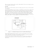


A51
GSP
The
A51
GSP
(graphics
system
processor)
provides
an
interface
between
the
A1
CPU
and
the
A52
LCD
.
The
A1
CPU
converts
the
formatted
data
to
GSP
commands
and
writes
them
to
the
A51
GSP
.
The
A51
GSP
processes
the
data
to
obtain
the
necessary
signals
and
sends
these
signals
to
the
A52
LCD
The
A51
GSP
receives
two
power
supply
voltages:
+5
VD
,
which
is
used
for
data
processing
and
converted
to
+3.3
V
,
and
+15
V
,
which
is
passed
on
the
A54
Inverter
.
The
+3.3
V
goes
to
the
A52
LCD
.
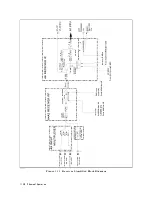
See
Figure
5-1
for
more
details
.
A54
Inverter
The
A54
Inverter
is
located
in
the
LCD
module
on
the
front
panel
assembly
.
The
A54
receives
+15
V
from
A1
CPU
and
provides
a
high
voltage
(800
to
1000
V
A
C)
to
the
backlight
of
the
LCD
.
See
Figure
5-1
for
more
details
.
A52
LCD
(Liquid
Crystal
Display)
The
A52
LCD
is
a
8.4
TFT
Color
LCD
,
receives
a
high
voltage
(800
to
1000
V
A
C)
from
the
A54
Inverter
as
backlight
power
and
the
digital
horizontal
and
the
vertical
signals
from
the
A51
GSP
.
A53
FDD
The
analyzer
has
a
built-in,
3-1/2
inch
FDD
(Flexible
Disk
Drive)
on
the
front
panel.
It
uses
2
high
density
or
2
double
density
3-1/2
inch
exible
disks
.
The
A53
FDD
stores
and
retrieves
data
to
and
from
the
disk.
Theory
of
Operation
11-13
Summary of Contents for Agilent 4396B
Page 10: ......
Page 32: ......
Page 43: ...Figure 2 7 CAL OUT Level Adjustment Location Adjustments and Correction Constants 2 11 ...
Page 46: ...Figure 2 10 Comb Generator Output 2 14 Adjustments and Correction Constants ...
Page 62: ...Figure 2 26 Final Gain Adjustment Location 2 30 Adjustments and Correction Constants ...
Page 76: ...Figure 3 1 Troubleshooting Organization 3 2 T roubleshooting ...
Page 84: ......
Page 90: ...Figure 5 1 Power Supply Lines Simpli ed Block Diagram 5 2 Power Supply T roubleshooting ...
Page 107: ...Figure 5 12 Power Supply Block Diagram 1 Power Supply T roubleshooting 5 19 ...
Page 108: ...Figure 5 13 Power Supply Block Diagram 2 5 20 Power Supply T roubleshooting ...
Page 109: ...Figure 5 14 Power Supply Block Diagram 3 Power Supply T roubleshooting 5 21 ...
Page 110: ......
Page 112: ...Figure 6 1 Digital Control Group Simpli ed Block Diagram 6 2 Digital Control T roubleshooting ...
Page 124: ......
Page 126: ...Figure 7 1 Source Group Block Diagram 7 2 Source Group T roubleshooting ...
Page 160: ...Figure 8 1 Receiver Group Simpli ed Block Diagram 8 2 Receiver Group T roubleshooting ...
Page 168: ......
Page 184: ...Figure 10 6 External Test Setup 1 Figure 10 7 External Test Setup 2 10 10 Service Key Menus ...
Page 185: ...Figure 10 8 External Test Setup 3 Figure 10 9 External Test Setup 4 Service Key Menus 10 11 ...
Page 226: ...Figure 11 3 Power Supply Functional Group Simpli ed Block Diagram 11 6 Theory of Operation ...
Page 231: ...Figure 11 5 Digital Control Group Simpli ed Block Diagram Theory of Operation 11 11 ...
Page 235: ...Figure 11 6 Source Simpli ed Block Diagram Theory of Operation 11 15 ...
Page 244: ...Figure 11 7 Receiver Simpli ed Block Diagram 11 24 Theory of Operation ...
Page 249: ...Figure IDC5S11001 here Figure 11 8 4396B Source Group Block Diagram Theory of Operation 11 29 ...
Page 254: ...Figure 12 1 Top View Major Assemblies 12 4 Replaceable Parts ...
Page 290: ...Figure 12 36 Main Frame Assembly Parts 17 19 12 40 Replaceable Parts ...
Page 294: ......
Page 308: ......
Page 311: ...Figure C 1 Power Cable Supplied Power Requirement C 3 ...
Page 312: ......
Page 324: ......


