
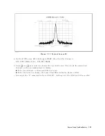


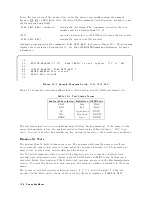


T
able
8-3.
A9J13
Pin
Description
Pin
Description
1
+15
V
P
ower
Supply
2
015
V
P
ower
Supply
3
R
Input
Select
(TTL
Level)
4
A
Input
Select
(TTL
Level)
5
B
Input
Select
(TTL
Level)
6
through
8
GND
(0
V)
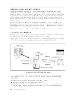
c.
Press
4
Meas
5 ,
N
NNNN
R
to
select
the
R
input.
Then
measure
the
voltages
at
pins
3,
4,
and
5
of
A9J13
using
an
oscilloscope
.
Check
that
the
measured
values
are
within
the
limits
.
The
typical
voltages
are
listed
in
T
able
8-4 .
If
the
voltages
are
good,
continue
with
the
next
step
.
If
the
voltages
are
bad,
inspect
the
cable
between
A9J13
and
A20J14.
If
the
cable
is
good,
the
A6
receiver
IF
is
probably
faulty
.
Replace
A6.
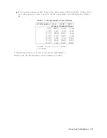
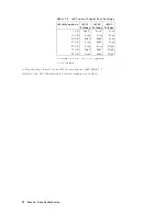
T
able
8-4.
A9
Control
Signal
T
est
Settings
Input
A9J13
Pin
3
A9J13
Pin
4
A9J13
Pin
5
R
High
1
Low
2
Low
A
Low
High
Low
B
Low
Low
High
1
is
typically
+5
V
(TTL
level).
2
is
typically
0
V
(TTL
Level).
d.
Change
the
input
in
accordance
with
T
able
8-4 .
Repeat
step
c
for
each
setting.
If
all
of
checks
above
are
good,
the
A9
control
signals
are
veried.
8-8
Receiver
Group
T
roubleshooting
Summary of Contents for Agilent 4396B
Page 10: ......
Page 32: ......
Page 43: ...Figure 2 7 CAL OUT Level Adjustment Location Adjustments and Correction Constants 2 11 ...
Page 46: ...Figure 2 10 Comb Generator Output 2 14 Adjustments and Correction Constants ...
Page 62: ...Figure 2 26 Final Gain Adjustment Location 2 30 Adjustments and Correction Constants ...
Page 76: ...Figure 3 1 Troubleshooting Organization 3 2 T roubleshooting ...
Page 84: ......
Page 90: ...Figure 5 1 Power Supply Lines Simpli ed Block Diagram 5 2 Power Supply T roubleshooting ...
Page 107: ...Figure 5 12 Power Supply Block Diagram 1 Power Supply T roubleshooting 5 19 ...
Page 108: ...Figure 5 13 Power Supply Block Diagram 2 5 20 Power Supply T roubleshooting ...
Page 109: ...Figure 5 14 Power Supply Block Diagram 3 Power Supply T roubleshooting 5 21 ...
Page 110: ......
Page 112: ...Figure 6 1 Digital Control Group Simpli ed Block Diagram 6 2 Digital Control T roubleshooting ...
Page 124: ......
Page 126: ...Figure 7 1 Source Group Block Diagram 7 2 Source Group T roubleshooting ...
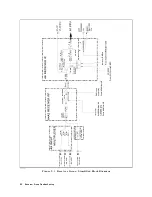
Page 160: ...Figure 8 1 Receiver Group Simpli ed Block Diagram 8 2 Receiver Group T roubleshooting ...
Page 168: ......
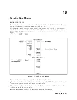
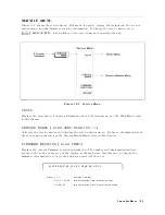
Page 184: ...Figure 10 6 External Test Setup 1 Figure 10 7 External Test Setup 2 10 10 Service Key Menus ...
Page 185: ...Figure 10 8 External Test Setup 3 Figure 10 9 External Test Setup 4 Service Key Menus 10 11 ...
Page 226: ...Figure 11 3 Power Supply Functional Group Simpli ed Block Diagram 11 6 Theory of Operation ...
Page 231: ...Figure 11 5 Digital Control Group Simpli ed Block Diagram Theory of Operation 11 11 ...
Page 235: ...Figure 11 6 Source Simpli ed Block Diagram Theory of Operation 11 15 ...
Page 244: ...Figure 11 7 Receiver Simpli ed Block Diagram 11 24 Theory of Operation ...
Page 249: ...Figure IDC5S11001 here Figure 11 8 4396B Source Group Block Diagram Theory of Operation 11 29 ...
Page 254: ...Figure 12 1 Top View Major Assemblies 12 4 Replaceable Parts ...
Page 290: ...Figure 12 36 Main Frame Assembly Parts 17 19 12 40 Replaceable Parts ...
Page 294: ......
Page 308: ......
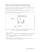
Page 311: ...Figure C 1 Power Cable Supplied Power Requirement C 3 ...
Page 312: ......
Page 324: ......


