


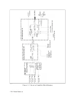


Single-Loop
Operation
at
Frequency
Spans
>
45
MHz.
In
the
single-loop
mode
,
the
V
CO
signal
loops
back
to
the
phase
detector
through
the
1/4
divider
and
the
1/16
divider
.
The
V
CO
frequency
(
F
vco
)
is
divided
by
64
and
then
compared
with
the
FRA
C
N
OSC
signal
frequency
(F
frac
)
(31.25
MHz
to
62.5
MHz)
in
the
phase
detector
.
Phase
locking
imposes
the
condition
of
F
frac
=
F
vco
/64.
Therefore
,
the
output
frequency
(F
vco
)
is
locked
to
F
frac
x
64.
The
F
vco
sweeps
from
2
GHz
(31.25
MHz
x
64)
to
4
GHz
(62.5
MHz
x
64)
according
to
the
FRA
C
N
OSC;
swept
signal.
The
frequency
range
actually
used
in
the
analyzer
is
2.05858
GHz
(at
a
measurement
frequency
0
Hz)
to
3.85858
GHz
(at
a
measurement
frequency
1.82
GHz).
Triple-Loop
Operation
at
Frequency
Spans
45
MHz.
In
the
triple-loop
mode
,
the
V
CO
signal
loops
back
to
the
phase
detector
through
the
1/4
divider
and
the
mixer
.
The
V
CO
frequency
(F
vco
)
is
mixed
with
the
STEP
OSC
output
(F
step
)
in
the
mixer
.
The
mixer
then
produces
the
shifted
frequency
of
F
vco
/4
-
F
step
.
The
mixer
output
is
compared
with
the
FRA
C
N
OSC
output
signal
in
the
phase
detector
.
Phase
locking
imposes
the
condition
of
F
frac
=
F
vco
/4
-
F
step
.
Therefore
,
the
output
frequency
F
vco
is
locked
to
F
frac
x
4
+
F
step
x
4.
The
F
vco
sweeps
over
the
appropriate
range
determined
by
the
start
and
stop
setting
according
to
the
F
frac
.
The
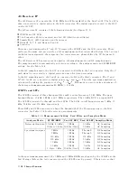
F
step
is
determined
by
the
center
frequency
of
the
analyzer
as
shown
in
T
able
11-1 .
The
F
frac
sweeps
between
f (start
frequency
+
2.05858
GHz)/4
-
F
step
g /4
to
f (stop
frequency
+
2.05858
GHz)/4
-
F
step
g /4.
Digital
Control
Signals
for
the
A4A2
Receiver
RF
The
A4A2
1st
LO
has
the
decoder
circuitry
for
the
following
digital
control
signals
.
These
signals
come
from
the
A1
CPU
.
The
decoded
signals
are
supplied
to
the
A4A2
Receiver
RF
through
the
cable
at
A4A1J2.
NA/SA
Switch
Control
Signal
AZ
(A
uto
Zero)
Control
Signal
A3A1
ALC
The
A3A1
ALC
generates
the
level-controlled
21.42
MHz
IF
signal,
an
8
MHz
reference
signal,
and
a
40
kHz
reference
signals
.
The
21.42
MHz
signal
is
supplied
to
the
A3A2
2nd
LO
and
converted
to
a
2.05858
GHz
IF
signal
through
the
source
rst
converter
.
The
8
MHz
and
40
kHz
signals
are
supplied
to
the
A6
receiver
IF
and
used
as
reference
signals
.
The
A3A1
ALC
consists
of
the
following
circuits:
Divider
Source
OSC
(Source
Oscillator)
ALC
(A
utomatic
Leveling
Control)
Divider
The
divider
contains
a
1/5
divider
and
a
1/200
divider
.
The
40
MHz
reference
frequency
from
the
A5
synthesizer
is
down
converted
to
8
MHz
and
40
kHz
through
the
two
dividers
.
The
two
signals
are
then
supplied
to
the
A6
receiver
IF
through
the
A20
motherboard.
Source
OSC
The
source
OSC
(source
oscillator)
is
a
phase
locked
oscillator
.
The
output
signal
is
phase
locked
to
the
40
kHz
frequency
of
the
divider
output.
The
oscillator
generates
the
85.68
MHz
signal.
The
signal
divided
by
the
1/4
divider
.
The
resulting
21.42
MHz
signal
is
supplied
to
the
ALC
circuit.
Theory
of
Operation
11-19
Summary of Contents for Agilent 4396B
Page 10: ......
Page 32: ......
Page 43: ...Figure 2 7 CAL OUT Level Adjustment Location Adjustments and Correction Constants 2 11 ...
Page 46: ...Figure 2 10 Comb Generator Output 2 14 Adjustments and Correction Constants ...
Page 62: ...Figure 2 26 Final Gain Adjustment Location 2 30 Adjustments and Correction Constants ...
Page 76: ...Figure 3 1 Troubleshooting Organization 3 2 T roubleshooting ...
Page 84: ......
Page 90: ...Figure 5 1 Power Supply Lines Simpli ed Block Diagram 5 2 Power Supply T roubleshooting ...
Page 107: ...Figure 5 12 Power Supply Block Diagram 1 Power Supply T roubleshooting 5 19 ...
Page 108: ...Figure 5 13 Power Supply Block Diagram 2 5 20 Power Supply T roubleshooting ...
Page 109: ...Figure 5 14 Power Supply Block Diagram 3 Power Supply T roubleshooting 5 21 ...
Page 110: ......
Page 112: ...Figure 6 1 Digital Control Group Simpli ed Block Diagram 6 2 Digital Control T roubleshooting ...
Page 124: ......
Page 126: ...Figure 7 1 Source Group Block Diagram 7 2 Source Group T roubleshooting ...
Page 160: ...Figure 8 1 Receiver Group Simpli ed Block Diagram 8 2 Receiver Group T roubleshooting ...
Page 168: ......
Page 184: ...Figure 10 6 External Test Setup 1 Figure 10 7 External Test Setup 2 10 10 Service Key Menus ...
Page 185: ...Figure 10 8 External Test Setup 3 Figure 10 9 External Test Setup 4 Service Key Menus 10 11 ...
Page 226: ...Figure 11 3 Power Supply Functional Group Simpli ed Block Diagram 11 6 Theory of Operation ...
Page 231: ...Figure 11 5 Digital Control Group Simpli ed Block Diagram Theory of Operation 11 11 ...
Page 235: ...Figure 11 6 Source Simpli ed Block Diagram Theory of Operation 11 15 ...
Page 244: ...Figure 11 7 Receiver Simpli ed Block Diagram 11 24 Theory of Operation ...
Page 249: ...Figure IDC5S11001 here Figure 11 8 4396B Source Group Block Diagram Theory of Operation 11 29 ...
Page 254: ...Figure 12 1 Top View Major Assemblies 12 4 Replaceable Parts ...
Page 290: ...Figure 12 36 Main Frame Assembly Parts 17 19 12 40 Replaceable Parts ...
Page 294: ......
Page 308: ......
Page 311: ...Figure C 1 Power Cable Supplied Power Requirement C 3 ...
Page 312: ......
Page 324: ......


