


Hardware and Software Configuration
Appendix C
GPIB-410 User Manual
C-2
© National Instruments Corp.
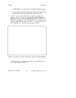
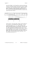
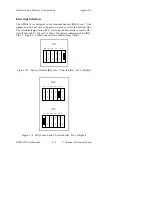
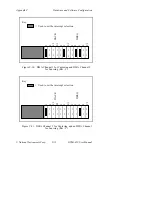
Figure C-1 shows the portion of the parts locator diagram with the base
I/O address switches (U49), the DMA channel jumpers (W1 and W2),
and the interrupt jumpers (W3).
Figure C-1. GPIB-410 Parts Locator Diagram (Rev. B.2 or Higher)
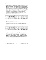
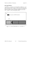
Base I/O Address Configuration
The GPIB-410 is addressed as an I/O port and decodes the lower ten
address lines of the PC I/O channel.
The base I/O address for the GPIB-410 is determined by the switches at
position U49 on the interface board. The switches are set at the factory
for the I/O port address 300 hex. This is used as the default base I/O
address value by the GPIB-410 software. The GPIB-410 occupies 32
contiguous bytes of I/O space. The base address of this 32-byte block of
addresses can be any multiple of 20 hex ranging from 000 hex to 3E0


