


Chapter 2
Hardware and Software Installation
© National Instruments Corp.
2-3
GPIB-410 User Manual
connector until the IEEE-488 connector is sticking out of the cut-
out. Slowly push down on the front of the GPIB-410 until the card
is level again. Lower the card until its edge connector is resting on
the expansion slot receptacle. Using an evenly distributed
pressure, press the GPIB-410 straight down until it seats in the
expansion slot.
7.
Re-install the bracket-retaining screw to secure the GPIB-410 to
the back-panel rail.
8.
If you wish to install the BNC I/O panel and cables for BNC trigger
output and BNC external clock input, you must locate another open
expansion slot for the panel. This panel does not require a full-
length slot.
9.
Locate and remove the bracket that covers the cut-out in the back
panel for the slot you have selected.
10.
Install the GPIB-410 BNC I/O panel into this slot and re-install the
bracket-retaining screw to secure it to the back panel rail.
11.
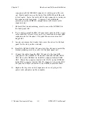
Connect the cables from the BNC I/O panel to the round RF
connectors on the GPIB-410. Match the connector labeled TRIG
OUT (J2) on the GPIB-410 to the BNC connector labeled TRIG
OUT. Match the connector labeled CLK IN (J3) on the GPIB-410
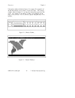
to the BNC connector labeled CLK IN. Figure 2-1 shows the BNC
I/O panel and cables connected to the GPIB-410 interface board.
12.
Replace the top cover and/or expansion slot cover, plug in the
power cord, and power up the computer.


