TM 11-6625-3071-14
3478A
the amplifier is then measured and stored into memory.
This reading is then subtracted from the DC Volts, DC
Current, and Ohms readings that follow. If the AC Volts
or AC Current Functions is selected, the zero reading is
taken differently. The input to the A/D Con- verter is
shorted to ground instead of the DC/Ohms In- put
Amplifier.
7-F-7. THEORY OF OPERATION
7-F-8. General
7-F-9. The following paragraphs give a detailed
description of the operating circuitry in the 3478A. The
circuitry is explained as follows:
a.
Input Circuitry - paragraph 7-F-10.
b.
Ohms Current Source - paragraph 7-F-17.
c.
AC to DC Converter - paragraph 7-F-25.
d.
A/D Converter - paragraph 7-F-31.
e.
3478A Logic Circuitry - paragraph 7-F-50.
f.
Chassis Common Circuitry - paragraph 7-F-55.
g.
Isolation Logic - paragraph 7-F-71.
h.
Floating Common Logic Circuitry paragraph 7-F-
75.
i.
Power Supplies - paragraph 7-F-83.
7-F-10. Input Circuitry
7-F-11. General. The purpose of the Input Circuitry is to
condition the dc input signals to the 3478A to provide full
scale 10V dc input voltages to the A/D Converter, for full
scale inputs to the 3478A (the explanation for ac inputs
is in paragraph 7-F-25, AC to DC Converter). The Input
Circuitry also acts as a buffer between the in- put and the
A/D Converter. The cicuitry can be separated (and is
explained) as follows:
Overvoltage
Protection Input Switching
Autozero and Pre-Charge
Pre-Charge Stage
DC/Ohms Input Amplifier
7-F-12. Overvoltage Protection. This circuitry has
three parts: High Voltage Protection, Low Voltage
Protec- tion, and Current Protection. The two circuits
operate as follows (refer to Schematic I for the
explanation).
a. High Voltage Protection. This circuit consist of a
630V Surge Voltage Protector (E101) in series with a
220K ohm resistor. The circuitry is connected between
the HI and LO INPUT Terminals and conducts with a
peak voltage level of 630V (+ 20%), which provides a low
impedance path across the terminals. Capacitor C104
provides a temporary low impedance path and R109
provides current limiting, if E101 conducts continuously.
b. Low Voltage Protection. This circuit consists
of diodes connected to the individual input nodes (part of
the HI INPUT, LO INPUT, A INPUT Paths, etc.). The
diodes on each node are connected (internally in U 102)
to + 3.5V and -3.5V power supplies. If the voltage on a
node exceeds 4.2V or -4.2V, a diode conducts
and keeps the level on the node to the + 4.2V levels.
The difference between the high voltage at the input ter-
minals and the voltage at the input nodes is dropped
across the resistors which are in series with the diodes
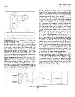
and input terminals (the low pass filter). Figure 7-F-2A
shows a typical protection circuit.
c.
Current Protection. A fuse in series with the
cur- rent shunt (RI01) protects the shunt from excessive
in- put currents (>3A). The fuse also opens if a voltage
greater than 250V is applied between the A and INPUT
LO Terminals.
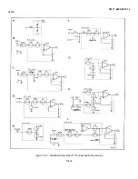
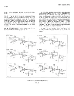
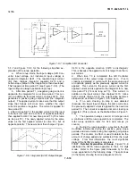
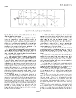
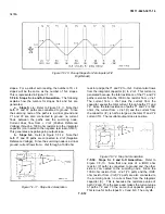
7-F-13. Input Switching. The Input Switching Circuitry
consists mostly of Relay and MOSFET switches, with
most FET switches located in U102. The purposes of
the switches are to provide five signal paths to the Input
Amplifier and to connect the amplifier for a zero
measurement (done in the Autozero Function; see
paragraph 7-F-14). The switches are controlled by
circuits in U102 which receive their control information
from the A/D Controller. The following explains the
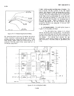
various input path,. Refer to Figure 7-F-2 and Schematic
1 for the explanation.
a.
Low Voltage Range Input Path (Figure 7-F-
2B). The path consists of K101, R103, R104, R10, and
SIDC (SIDC is in U102). The purpose of the path is to
connect the HI INPUT Terminal (high input voltage) to
the DC/Ohms Input Amplifier. The path is used only in
the 30mV through 3V dc volts Ranges and all Ohms
Ranges.
b. High Voltage Range Input Path (Figure 7-F-
2C). The path consists of RI 10, K102, S2DC (in 102),
and a 100:1 divider (9.9M ohm and 100K ohm resistors,
RD99 and RD98, in U102). The purpose of the path is to
attenuate input voltages by a facter of 100 and to
connect the attenuated voltage to the DC/Ohms Input
Amplifier. The path is used only in the 30V and 300V dc
volts Ranges.
c.
Ohms High Sense Path (Figure 7-F-2D). This
path consists of RIOS, R106, and S4ADC and S4BDC
(S4ADC and S4BDC are in U102). The path connects
the HI OHMS SENSE Terminal (high ohms input) to the
DC/Ohms Input Amplifier, only when the 3478A is in the
4-Wire Ohms Function. Switch S4CDC (which is also
part of the path) is used to connect the junction of
S4ADC and S4BDC to ground. Switch S4CDC is closed
in all functions except the 4-Wire Ohms Function and
shunts any possible voltage on the S4ADC and S4BDC
junction to ground.
7-F-3
Содержание 3478A
Страница 2: ...TM 11 6625 3071 14 A ...
Страница 4: ...TM 11 6625 3071 14 C D BLANK ...
Страница 12: ...TM 11 6625 3071 14 Table 1 1 Specification 1 2 ...
Страница 13: ...TM 11 6625 3071 14 Table 1 1 Specifications Cont 1 3 ...
Страница 14: ...TM 11 6625 3071 14 Table 1 1 Specifications Cont 1 4 ...
Страница 53: ...TM 11 6625 3071 14 1 ...
Страница 54: ...TM 11 6625 3071 14 2 ...
Страница 55: ...TM 11 6625 3071 14 3 ...
Страница 56: ...TM 11 6625 3071 14 4 ...
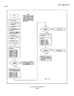
Страница 87: ...TM 11 6625 3071 14 3478A Figure 7 D 3 Flowchart B 7 D 5 ...
Страница 88: ...TM 11 6625 3071 14 3478A Figure 7 D 4 Flowchart C 7 D 6 ...
Страница 91: ...TM 11 6625 3071 14 3478A Figure 7 D 6 Flowchart D 7 D 9 ...
Страница 98: ...TM 11 6625 3071 14 3478A Figure 7 F 2 Simplified Schematic Of The Input Switching Circuitry 7 F 4 ...
Страница 111: ...TM 11 6625 3071 14 Figure 7 F 17 3478A Simplified Reference Circuitry 7 F 16 ...
Страница 122: ...TM 11 6625 3071 14 Table A 2 A 2 HP IB Worksheet A 4 ...
Страница 137: ...TM 11 6625 3071 14 Figure 7 D 2 Flow chart A 7 D 3 ...
Страница 139: ...TM 11 6625 3071 14 Figure 7 G 2 3478A Block Diagram 7 G 3 ...
Страница 140: ...TM 11 6625 3071 14 Component Locator for Input Circuitry and Ohms Current Source 7 G 4 ...
Страница 141: ...TM 11 6625 3071 14 Figure 7 G 3 Input Circuitry and Ohms Current Source 7 G 5 ...
Страница 142: ...TM 11 6625 3071 14 F G 6 ...
Страница 143: ...TM 11 6625 3071 14 2 Figure 7 G 4 AC to DC Converter 7 G 7 ...
Страница 144: ...TM 11 6625 3071 14 Component Locator for A D Converter and Control Logic 7 G 8 ...
Страница 145: ...TM 11 6625 3071 14 3 Figure 7 G 5 A D Converter and Control Logic 7 G 9 ...
Страница 146: ...TM 11 6625 3071 14 7 G 10 ...
Страница 147: ...TM 11 6625 3071 14 4 Figure 7 G 6 Power Supplies 7 G 11 7 G 12 blank ...
Страница 148: ......
Страница 149: ...PIN NO 057444 ...


