TM 11-6625-3071-14
3478A
b.
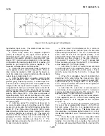
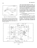
If it has been determined that the remaining
voltage on the integrator is negative, S-4 currents are
applied a number of times until zero crossing occurs
(CMP output changes state). Since the S-4 currents can
be applied (during time TI in Figure 7-F-14) to a
maximum of three ramps, the resultant output slope S-4
will normally cross zero with three or less S-4 currents
applied. After zero crossing occurs, the current is
removed with 15 ALE cycles (i.e. one half-ramp) after
the S-4 slope crosses zero. If (after the current is
removed) time TI is not completed, a no current
condition remains (i.e. an S-O slope) for the rest of time
TI. No current is applied to keep the rundown time
constant.
c.
If the remaining voltage on the integrator is
positive, current S-4 is applied for a short time and then
removed. The current is applied for a short time
because the current develops a positive output slope and
the integrator voltage is also positive. Both the slope and
the integrator voltage together could saturate the
integrator. When Current S-4 is removed, no current (an
S-0 slope) is then applied for the rest of time T1. Cur-
rent S-4 is applied whether the integrator voltage is
positive or negative. This is to make sure that the slopes
that follow (slope S + 4) will always cross zero and that
the same transitions occurs for all readings.
d.
The next current applied is positive S + 4
current. Its value is the same as S-4, but in the opposite
direction. The current is applied until slope S+4 crosses
zero. The current can be applied (during time T2) a
maximum of three ramps. This makes time T2 the same
as time TI. The S+4 currents are also removed within 15
ALE cycles after the S+4 slope crosses zero. Here
again, no current is applied (slope S-0) for the re-
mainder of time T2.
e.
After time T2, the next current applied is
negative S-3 current (its polarity is opposite of S + 4).
Because the value of an S-3 current is 1/10 the value of
an S-4 cur- rent, the resultant S-3 slope is not as steep
and takes longer time to cross zero. This makes the
maximum number of times the currents can be applied
(during time T3) seven times instead of three. The S-3
current is also removed within 15 ALE cycles after slope
S-3 crosses zero. Then no current (S-0) is applied for
the re- mainder of time T3.
f.
When time T3 is completed, positive current S +
2 is applied. This current is 1/10 the value of S-3 (1/100
of S-4) and in the opposite direction. The maximum
number of times the S + 2 current can be applied is
seven (as are S-3 currents). Time T4 has the same
amount of time as T3. The S + 2 currents are also
removed within 15 ALE cycles after slope S+2 crosses
zero. Then no current (S-0) is applied for the remainder
of time T4.
g.
The next current applied is negative S-1. This
cur- rent is 1/10 the value of S+2 (1/1000 of S+4) and in
the opposite direction. The current is applied until it
crosses zero. The currents are also removed within 15
ALE cycles after slope S-I crosses zero.
h.
Once the S-I currents are removed a positive S
+ I current is applied for 5 ALE cycles and is called one
sixth ramp. This current is applied instead of no current
and only happens after the S-I slope. The current has -
the same value as S-l, but in the opposite direction. The
currents are applied until zero crossing occurs and are
removed within 5 ALE cycles after crossing zero.
i.
After current S+I is removed, within 5 ALE
cycles, current S-I is reapplied. This new S-I current is
also applied until zero crossing occurs. After S-I slope
cross zero, current S + 1 is reapplied. After current S + I
is removed, S-I is applied, and so on. This takes place
until time T5 (and rundown) is completed.
j.
During the rundown time, a counter in the A/D
Controller counts the number of S-4, S + 4, S-3, S + 2,
and S-1 slopes it takes for each set of slopes to cross
zero. This is then used to calculate the three least
significant digits of the 3478A’s reading.
7-F-46. Integrator Offset Compensation. The A/D
Integrator can have offsets which prevent the S + 2 and
S- 1 slopes from crossing zero. To make sure the
slopes will cross zero, the A/D’s DAC (Digital to Analog
Con- verter, U465 and associated circuitry) is turned on
before the S + 2 currents are applied. The DAC is used
to null out any offsets from the integrator. The maximum
number of times the S + 2 current can be applied is
seven (as are S-3 currents). Time T4 has the same
amount of time as T3. The S + 2 currents are also
removed within 15 ALE cycles after slope S + 2 crosses
zero. Then no current (S-0) is applied for the remainder
of time T4.
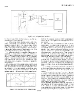
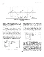
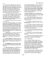
7-F-47. The correct DAC setting is determined during
the time when the S+ I and S-I currents are applied.
These currents are applied after the first set of S-I slopes
have crossed zero (see paragraph 7-F-45, step g).
Since both S+ 1 and S-I currents have the same
amplitude, the S + I and S-l slopes should have the same
magnitude (i.e. zero crossing should occur at a a certain
time). If a difference in magnitude is noted by the A/D
Controller, the DAC is adjusted until the magnitude of the
S + I and S-I slopes are the same. This is illustrated in
Figure 7-F-15.
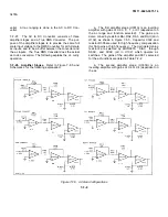
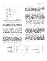
7-F.48. Rundown Slope Generation. The S-4 and S +
4 slopes are generated the same way it is done for the
runup operation (see paragraphs 7-F-38). The only dif-
ference is that they only depend on the applied S-4 and
S +4 currents, not the input current. The S-O slope is
generated the same way as the S-0 slope in runup (see
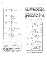
paragraph 7-F-39). The S-3 and S-1 currents use the
same circuitry configuration as the S-4 current (see x H ·
Figure 7-F-12), but use different resistor values. The
resistor values are such that the S-3 current is 1/10 the
7-F-14
Содержание 3478A
Страница 2: ...TM 11 6625 3071 14 A ...
Страница 4: ...TM 11 6625 3071 14 C D BLANK ...
Страница 12: ...TM 11 6625 3071 14 Table 1 1 Specification 1 2 ...
Страница 13: ...TM 11 6625 3071 14 Table 1 1 Specifications Cont 1 3 ...
Страница 14: ...TM 11 6625 3071 14 Table 1 1 Specifications Cont 1 4 ...
Страница 53: ...TM 11 6625 3071 14 1 ...
Страница 54: ...TM 11 6625 3071 14 2 ...
Страница 55: ...TM 11 6625 3071 14 3 ...
Страница 56: ...TM 11 6625 3071 14 4 ...
Страница 87: ...TM 11 6625 3071 14 3478A Figure 7 D 3 Flowchart B 7 D 5 ...
Страница 88: ...TM 11 6625 3071 14 3478A Figure 7 D 4 Flowchart C 7 D 6 ...
Страница 91: ...TM 11 6625 3071 14 3478A Figure 7 D 6 Flowchart D 7 D 9 ...
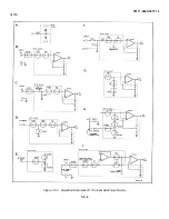
Страница 98: ...TM 11 6625 3071 14 3478A Figure 7 F 2 Simplified Schematic Of The Input Switching Circuitry 7 F 4 ...
Страница 111: ...TM 11 6625 3071 14 Figure 7 F 17 3478A Simplified Reference Circuitry 7 F 16 ...
Страница 122: ...TM 11 6625 3071 14 Table A 2 A 2 HP IB Worksheet A 4 ...
Страница 137: ...TM 11 6625 3071 14 Figure 7 D 2 Flow chart A 7 D 3 ...
Страница 139: ...TM 11 6625 3071 14 Figure 7 G 2 3478A Block Diagram 7 G 3 ...
Страница 140: ...TM 11 6625 3071 14 Component Locator for Input Circuitry and Ohms Current Source 7 G 4 ...
Страница 141: ...TM 11 6625 3071 14 Figure 7 G 3 Input Circuitry and Ohms Current Source 7 G 5 ...
Страница 142: ...TM 11 6625 3071 14 F G 6 ...
Страница 143: ...TM 11 6625 3071 14 2 Figure 7 G 4 AC to DC Converter 7 G 7 ...
Страница 144: ...TM 11 6625 3071 14 Component Locator for A D Converter and Control Logic 7 G 8 ...
Страница 145: ...TM 11 6625 3071 14 3 Figure 7 G 5 A D Converter and Control Logic 7 G 9 ...
Страница 146: ...TM 11 6625 3071 14 7 G 10 ...
Страница 147: ...TM 11 6625 3071 14 4 Figure 7 G 6 Power Supplies 7 G 11 7 G 12 blank ...
Страница 148: ......
Страница 149: ...PIN NO 057444 ...

