TM 11-6625-3071-14
3478A
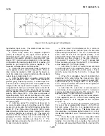
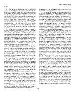
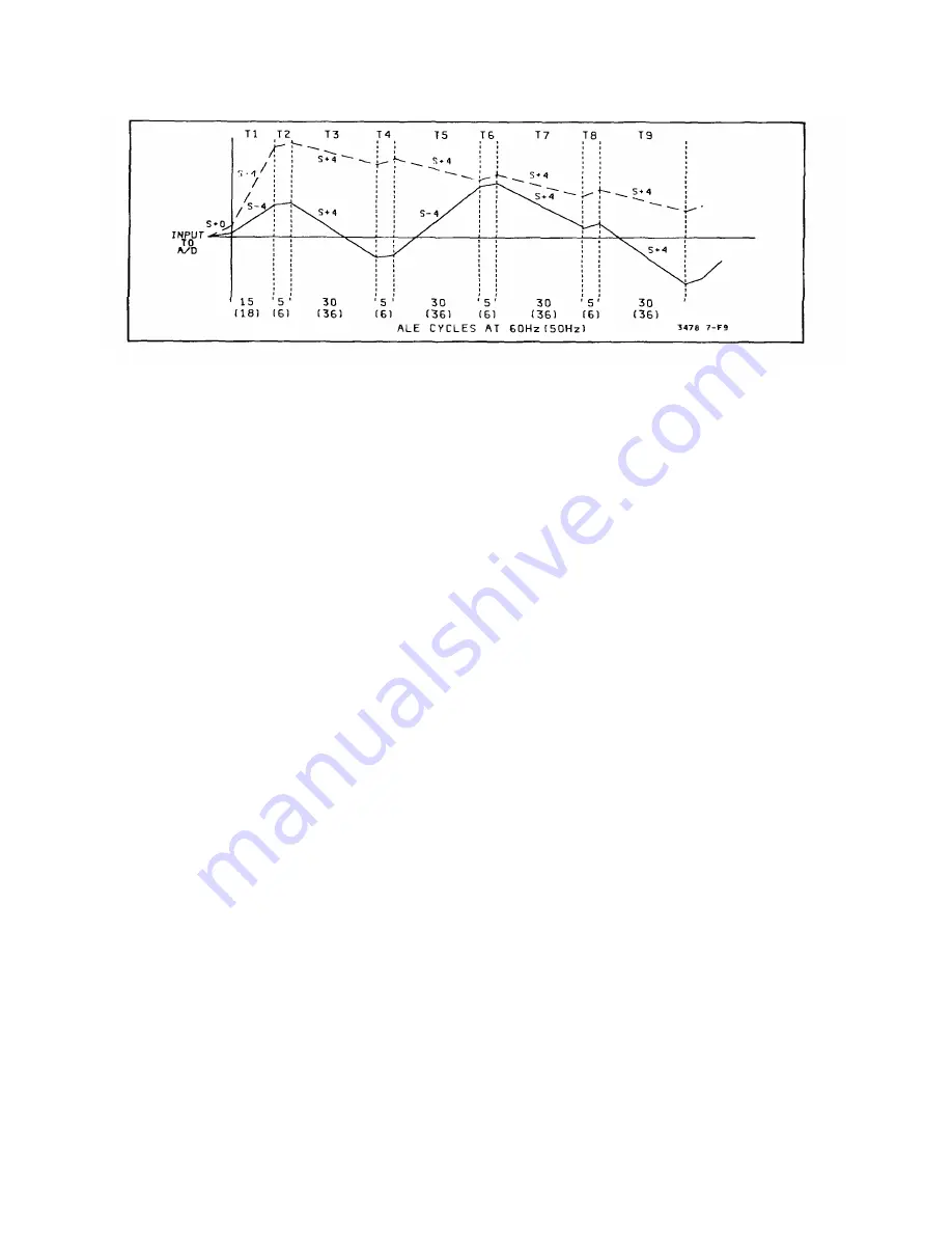
Figure 7-F-9. Runup Slopes (4 ½ Digit Model)
hypothetical input value. The dashed lines are for a
larger hypothetical input value.
a.
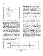
When runup starts, the integrator capacitor
(C410) is charged by the input current (which is
developed by the input voltage). The input current is
applied to the negative terminal of integrator U401 (see
Figure 7-F-7), and since the integrator is in the inverting
configuration, the resultant output of U401 is positive (for
positive in- put currents the slope is negative). The
capacitor is charged for a short time period.
b.
During the time period when only the input cur-
rent is applied, no other currents charge C410. Since no
other current is applied to U401 (except the input cur-
rent), it is called a no current condition and the resultant
output slope is called slope S + 0.
c.
After the time period, a negative current (called
S-4) is then applied to U401. This current develops a
positive going output slope which is called slope S-4.
The S4 current is always the first current applied to the
integrator after the input current is applied. The current
is applied for 15 ALE cycles (18 ALE cycles in the 50 Hz
option) and is for time period TI. Since the input cur- rent
and the applied current in the example have the same
polarity, both charge C410. If the input current was at
opposite polarity, C410 will still be charged in the same
direction but the output slope will be less steep. This is
because the applied current (S-4) is normally larger than
the input current.
d.
After time period TI, current S-4 is removed. A
no current condition (slope S-O) will then exist for 5 ALE
cycles (or 6 ALE cycles for the 50Hz option) during time
period T2. The charge rate of Capacitor C410 is again
determined by only the input current. Slope S-O is also a
no current condition, as is slope S + 0. The major dif-
ference is that the slopes are generated differently (see
paragraph 7-F-39). Slope S-O is selected since the
previous no current condition was slope S + 0. The
slopes alternate with each other (S + 0, S-O, S + 0, etc.)
for each no current condition.
e.
When time T2 is completed, an S + 4 current is
applied for 30 ALE cycles (36 ALE cycles for the 50Hz
option) during time period T3. The S + 4 current has the
same value as S-4, but at opposite polarity. This
charges C410 in the other direction (i.e. the capacitor is
discharged and then charged in the other direction).
Time period T3, and the TS, T7, and T9 periods that
follow are twice as long as time period T1 (30 or 36 ALE
cycles instead of 15 or 18 ALE cycles).
f.
After time T3, the S +4 current is removed and
no current (slope S + 0) is applied for time T4. Time T4
is as long as time period T2 (5 or 6 ALE cycles). This is
also the same time for the S-O or S + 0 slopes that
follow.
g.
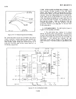
When T4 is completed, the A/D Controller then
determines if the output slope has crossed zero. Zero
crossing occurs when the A/D comparator’s output (CMP
output at U403 pin 11) changes state. In the example,
zero crossing is detected and current S-4 is applied for
time T5 (30 or 36 ALE cycles).
h.
After time TS, current S-4 is removed and no
current (slope S-O) is applied for time T6. Since zero
crossing was detected (during time T5), current S + 4 is
applied for time T7, after slope S-0 is completed.
i.
When time T7 is completed, no current (slope S
+ 0) is applied for time T8. Since no zero crossing was
detected, current S + 4 is reapplied for time T9 (after
slope S + 0).
j.
Since zero crossing was detected during time
T9, current S-4 is applied (after slope S + 0) for 30 (or
36) ALE cycles. Then S + 4 is applied (since zero
crossing is detected) and so on. This takes place until
the runup time is completed (either current S + 4 or S-4
is selected, dependent upon if and when zero crossing
occurs).
k.
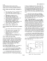
Once the runup operation is completed, U462
then determines the 2 most significant digits of the
reading. For other than a zero reading, the number of
S+4 slopes will always be different than the number of S-
4
7-F-11
Содержание 3478A
Страница 2: ...TM 11 6625 3071 14 A ...
Страница 4: ...TM 11 6625 3071 14 C D BLANK ...
Страница 12: ...TM 11 6625 3071 14 Table 1 1 Specification 1 2 ...
Страница 13: ...TM 11 6625 3071 14 Table 1 1 Specifications Cont 1 3 ...
Страница 14: ...TM 11 6625 3071 14 Table 1 1 Specifications Cont 1 4 ...
Страница 53: ...TM 11 6625 3071 14 1 ...
Страница 54: ...TM 11 6625 3071 14 2 ...
Страница 55: ...TM 11 6625 3071 14 3 ...
Страница 56: ...TM 11 6625 3071 14 4 ...
Страница 87: ...TM 11 6625 3071 14 3478A Figure 7 D 3 Flowchart B 7 D 5 ...
Страница 88: ...TM 11 6625 3071 14 3478A Figure 7 D 4 Flowchart C 7 D 6 ...
Страница 91: ...TM 11 6625 3071 14 3478A Figure 7 D 6 Flowchart D 7 D 9 ...
Страница 98: ...TM 11 6625 3071 14 3478A Figure 7 F 2 Simplified Schematic Of The Input Switching Circuitry 7 F 4 ...
Страница 111: ...TM 11 6625 3071 14 Figure 7 F 17 3478A Simplified Reference Circuitry 7 F 16 ...
Страница 122: ...TM 11 6625 3071 14 Table A 2 A 2 HP IB Worksheet A 4 ...
Страница 137: ...TM 11 6625 3071 14 Figure 7 D 2 Flow chart A 7 D 3 ...
Страница 139: ...TM 11 6625 3071 14 Figure 7 G 2 3478A Block Diagram 7 G 3 ...
Страница 140: ...TM 11 6625 3071 14 Component Locator for Input Circuitry and Ohms Current Source 7 G 4 ...
Страница 141: ...TM 11 6625 3071 14 Figure 7 G 3 Input Circuitry and Ohms Current Source 7 G 5 ...
Страница 142: ...TM 11 6625 3071 14 F G 6 ...
Страница 143: ...TM 11 6625 3071 14 2 Figure 7 G 4 AC to DC Converter 7 G 7 ...
Страница 144: ...TM 11 6625 3071 14 Component Locator for A D Converter and Control Logic 7 G 8 ...
Страница 145: ...TM 11 6625 3071 14 3 Figure 7 G 5 A D Converter and Control Logic 7 G 9 ...
Страница 146: ...TM 11 6625 3071 14 7 G 10 ...
Страница 147: ...TM 11 6625 3071 14 4 Figure 7 G 6 Power Supplies 7 G 11 7 G 12 blank ...
Страница 148: ......
Страница 149: ...PIN NO 057444 ...

