TM 11-6625-3071-14
3478A
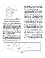
The flip-flop operates like a latch and transfers data from
Port P23 during each ALE cycle.
c. Once the previous conditions are met (the RAM is
addressed) and line CE2 is high, data from the RAM is
transferred to the Data Lines.
7-F-63. Sending Data to the RAM. The RAM can
receive new Data when its R/W line (Read/Write at U5
12 pin 20) is low. This can only happen if the 3478A’s
Cal Enable Switch (located on the front panel) is on and
the WR line of the CPU (Write at U501 pin 10) is low.
The following explains the operation.
a.
The Cal Enable Switch brings one input of NOR
gate U508C low.
b.
The other input of the gate is a low from the WR
line.
c.
The output of U508C goes high, and since NOR
gate U508D is configured as an inverter, the output of
U508D goes low. The RAM is now ready to receive new
data.
7-F-64. Since the 3478A’s Calibration Constants are
stored in the CMOS RAM, the constants must remain in
the RAM when the 3478A is turned off (or power
removed). This is done by battery BT701 in the + 5V
Power Supply Circuit. In addition, the RAM should not
see any possible write commands (R/W low) during the
time that power is removed. The RAM must be disabled.
This is because a write command may erase some
calibration constants. The RAM is disabled by
comparator U750C (part of the CPU’s power-on circuit in
the + 5V power supply). The operation is as follows
(refer to Schematic 4 for the explanation):
a.
As long as the 3478A is on, the RAM gets its
supply voltage from Q701.
b.
When power is off, the RAM gets its supply
voltage from battery BT701 through diode CR764. The
battery voltage is used for data retention.
c.
After turning power off, the RAM is disabled by
setting Line CE2 low. This is done by comparator
U750C. The comparator senses a low (or no + 5V) from
voltage divider R761, R762, and R763. Since U750OC’s
negative terminal is at the battery voltage, the output of
U70SOC becomes low. This makes line CE2 low and
disables the RAM.
7-F-65. Keyboard Operation. The Keyboard’s
pushbuttons are connected in a 4x4 matrix and are
continuously scanned by the CPU. The operation is as
follows:
a.
One side of the matrix is connected to Ports
P10O to P13 of the CPU (US01 pins 27 to 30) and the
other side is connected to Ports P14 to P17 (U501 pins
31 to 34).
b.
Before scanning starts, Ports P14 to P17 are
low. When scanning begins, starting with Port P14, each
port goes sequentially high.
c.
During the time that the keyboard is scanned,
the CPU determines which one and if any of Ports P0O
to P13 are high. A high on P10 to P13 is used to
determine the button pressed. For example, the SRQ
button is pressed and turns the corresponding SRQ
switch on. This connects Port P11 to P17 and makes
P11 high when P17 is high. Since the CPU knows when
it sets P17 high and also knows when P 11 is high, the
pressed button is determined.
7-F-66. Display Operation. The 3478A Display is an
alphanumeric display with 12 annunciators. The CPU
sends serial data to the Display Circuitry which in turn
does all the necessary decoding of the data (to display
readings, etc.). The operation is as follows:
a.
With line PWO high, the CPU can send new
data to the Display Circuitry. Data is in serial form and is
sent on the Data line (U506 pin 4). For the Display
Circuitry to receive and decode the data, the other
display lines have to send certain information to the
circuitry. This is as follows:
1.
The Display Circuitry requires two clock
inputs to receive data, I and 12. The inputs come
from flip-flop U506 (pin3) and Port P25 for clock
inputs 11 and 12, respectively. (Flip-flop U506 is
used as a latch between the CPU and the Display
Circuitry.)
2.
The ISA line (U506 pin 5) is used to give
instructions to the Display Circuitry.
3.
The SYNC line (U506 pin 6) is used to tell
the Display Circuitry when to look for instructions.
b.
With line PWO (from Port P23 of the CPU at
US01 pin 36) low, the Display Circuitry operates without
receiving any data from the CPU. The circuitry can
operate in this mode since it has an internal clock
(capacitor C502 is the frequency reference). With the
circuitry in the internal mode, no updating of the display
is done. Line PWO is controlled by the CPU.
7-F-67. HP-IB Operation. All interfacing between the
CPU and the Hewlett-Packard Interface Bus (HP-IB) is
done by the HP-IB Chip (U503) and two Bus
Transceivers (U504 and USOS). The HP-IB Chip is a
microprocessor and changes the data sent and received
by the CPU to the necessary HP-IB information (e.g.
Listen, Talk, etc.). The Transceivers transfer and
receive the HP-IB information between the HP-IB Chip
and the Bus. The circuitry operates as follows:
a. The HP-IB Chip (U503) receives its clock signal
from the CPU’s TO output (U501 pin 1).
7-F-19
Содержание 3478A
Страница 2: ...TM 11 6625 3071 14 A ...
Страница 4: ...TM 11 6625 3071 14 C D BLANK ...
Страница 12: ...TM 11 6625 3071 14 Table 1 1 Specification 1 2 ...
Страница 13: ...TM 11 6625 3071 14 Table 1 1 Specifications Cont 1 3 ...
Страница 14: ...TM 11 6625 3071 14 Table 1 1 Specifications Cont 1 4 ...
Страница 53: ...TM 11 6625 3071 14 1 ...
Страница 54: ...TM 11 6625 3071 14 2 ...
Страница 55: ...TM 11 6625 3071 14 3 ...
Страница 56: ...TM 11 6625 3071 14 4 ...
Страница 87: ...TM 11 6625 3071 14 3478A Figure 7 D 3 Flowchart B 7 D 5 ...
Страница 88: ...TM 11 6625 3071 14 3478A Figure 7 D 4 Flowchart C 7 D 6 ...
Страница 91: ...TM 11 6625 3071 14 3478A Figure 7 D 6 Flowchart D 7 D 9 ...
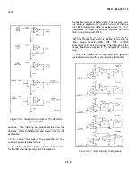
Страница 98: ...TM 11 6625 3071 14 3478A Figure 7 F 2 Simplified Schematic Of The Input Switching Circuitry 7 F 4 ...
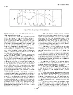
Страница 111: ...TM 11 6625 3071 14 Figure 7 F 17 3478A Simplified Reference Circuitry 7 F 16 ...
Страница 122: ...TM 11 6625 3071 14 Table A 2 A 2 HP IB Worksheet A 4 ...
Страница 137: ...TM 11 6625 3071 14 Figure 7 D 2 Flow chart A 7 D 3 ...
Страница 139: ...TM 11 6625 3071 14 Figure 7 G 2 3478A Block Diagram 7 G 3 ...
Страница 140: ...TM 11 6625 3071 14 Component Locator for Input Circuitry and Ohms Current Source 7 G 4 ...
Страница 141: ...TM 11 6625 3071 14 Figure 7 G 3 Input Circuitry and Ohms Current Source 7 G 5 ...
Страница 142: ...TM 11 6625 3071 14 F G 6 ...
Страница 143: ...TM 11 6625 3071 14 2 Figure 7 G 4 AC to DC Converter 7 G 7 ...
Страница 144: ...TM 11 6625 3071 14 Component Locator for A D Converter and Control Logic 7 G 8 ...
Страница 145: ...TM 11 6625 3071 14 3 Figure 7 G 5 A D Converter and Control Logic 7 G 9 ...
Страница 146: ...TM 11 6625 3071 14 7 G 10 ...
Страница 147: ...TM 11 6625 3071 14 4 Figure 7 G 6 Power Supplies 7 G 11 7 G 12 blank ...
Страница 148: ......
Страница 149: ...PIN NO 057444 ...

