TM 11-6625-3071-14
3478A
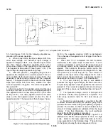
+ 8V, its inverting terminal must also be + 8V (the in-
verting terminal draws little or no current). This makes
the resultant voltage drop across the Range Res
4V (or + .4V for the 30M ohm Range).
d.
A current is then generated with its value
proportional to the value of the Range Resistor and the
voltage drop across the resistor.
e.
The current is applied to the unknown resistor
through the Output MOSFET (in U102), High Voltage
Protection Circuitry, and the HI INPUT Terminal. The
3478A’s Ohms Ranges, Ohms Currents, Range
Resistors, and selected MOSFET Switches are listed in
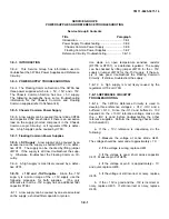
Table 7-F-1.
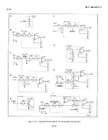
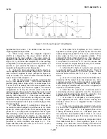
7-F-21. Voltage Splitter (U201). The following explains
the Voltage Splitter (Reference) Circuitry.
a.
The Voltage Splitter is a XI.5 gain non-inverting
amplifier with an output of + 12V (for the 300 ohm to 3M
ohm Ranges) or + 8.4V (for the 30M ohm Range).
b.
The gain is determined by feedback resistors
RR3, RR4 (both in U102), and R201. Since the total
value of RR3 plus RR4 is 20K ohm and R201 is 40K
ohm, the non-inverting gain is XI.5. (The gain is:
[20K/40K] + 1 = 1.5).
c.
The + 12V output is generated by ap8V
to the amplifier input (8*1.5 = 12). The +8V is deter-
mined by the + O1V Reference (from the 3478A’s
Reference Circuitry, see paragraph 7-F-49d) and voltage
divider RRO, RRI, and RR2. The sum of RRI and RR2 is
200K ohm and RRO is 50K ohm resulting in a voltage
drop across the resistors of + 8V and + 2V, respective-
ly. The + 8V is applied through FET Switch SOR to
U201.
d.
The + 8.4V output is generated by applying
+5.6V to the amplifier input (5.6*1.5=8.4). The + 5.6V is
also determined by the + O1V Reference (from the
3478A’s Reference Circuitry) and voltage divider RRO,
RRI, and RR2. In this case the voltage drop across RR2
(which is +5.6V developed across 140K ohm) is applied
through FET Switch SIR to U201.
7-F-22. Buffer (U202) and Range Resistors (RR5 to
RR8). The Buffer is a non-inverting XI gain amplifier with
its output at 12V or + 8.4V (on the 30M
ohm Range only). The gain is selected by either
MOSFET Switch pairs S6R and S7R, SS8R and S9R,
SIOR and SIIR, or S12R and S13R. The Range
Resistors are used to determine the different ohms cur-
rent values. Refer to Table 7-F-I to determine which
switch and resistor is selected for the different ohms
ranges.
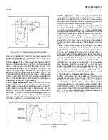
7-F-23. The Output FET Control Amplifier (U203) and
the Output MOSFET (in U102) form a feedback circuit
used to boost the output impedance of the Output
MOSFET. The FET is normally biased into saturation,
and in conjunction with the open loop gain of U203 and
the Range Resistors, results in a high output impedance
of the Ohms Current Source. A high output impedance
is necessary to prevent measurement nonlinearities.
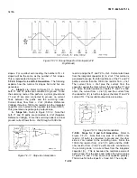
7-F-24. Overvoltage Protection Circuitry. The
circuitry is used to protect the Ohms Current Source
from high voltages inadvertently applied to the 3478A’s
Input Ter- minals (when the Multimeter is in the Ohms
Function). The following explains the circuitry operation.
a.
If a large positive voltage is applied to the
3478A’s HI INPUT Terminal, the voltage is applied
through R204 and L201 to the cathode of CR201. Since
the cathode voltage of CR201 is higher than the anode
voltage, the diode is reverse biased. This prevents the
large input voltage from damaging the current source.
b.
If a large negative voltage is applied to the
3478A’s HI INPUT Terminal, the voltage is dropped
across CR201, R203, and R202 to diode connected FET
Q205. This makes Q205 conduct and in turn clamps the
base of Q202 at -.7V (one diode drop). This voltage
along with negative collector to base voltage forces
Q201, Q202, Q203, and Q204 to turn on. Transistors
Q201 and Q203 conducts no more current than the
circuit which generates the ohms current (on a given
range). The cir- cuit that generates the ohms current
cannot tell the dif- ference between a valid unknown
resistance and the large negative input voltage. Most of
the large input voltage is dropped across R202 and
R203.
7-F-25. AC to DC Converter
7-F-26. The purpose of the AC to DC Converter is to
convert the 3478A’s ac inputs (volts or current) to dc
volts. The converter output is + 3.00000V dc for all full-
scale ac inputs with the output applied to the A/D Con-
Table 7-F-1. Ohms Current and Ranges
Ohms
Ohms
Range
Resistor
FET Switches
Range
Current
Resistor
Voltage
Enabled
300-3K
1mA
4K (RR5)
4V
SOR.S2R,S3R,S6R,S7R.S14R
30K
.1mA
40K (RR6)
4V
SOR,S2R,S3R.SSR,S9R,S9R,S14R
300K
.01mA
400K (RR7)
4V
SOR,S2R,S4R,S1OR.S11R
3M
1uA
4M (RR8)
4V
SOR,S2R,12R,S13R
30M
.1uA
4M (RR8)
.4V
S1R,S5R,S12R,S13R
7-F-7
Содержание 3478A
Страница 2: ...TM 11 6625 3071 14 A ...
Страница 4: ...TM 11 6625 3071 14 C D BLANK ...
Страница 12: ...TM 11 6625 3071 14 Table 1 1 Specification 1 2 ...
Страница 13: ...TM 11 6625 3071 14 Table 1 1 Specifications Cont 1 3 ...
Страница 14: ...TM 11 6625 3071 14 Table 1 1 Specifications Cont 1 4 ...
Страница 53: ...TM 11 6625 3071 14 1 ...
Страница 54: ...TM 11 6625 3071 14 2 ...
Страница 55: ...TM 11 6625 3071 14 3 ...
Страница 56: ...TM 11 6625 3071 14 4 ...
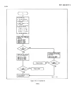
Страница 87: ...TM 11 6625 3071 14 3478A Figure 7 D 3 Flowchart B 7 D 5 ...
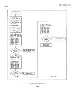
Страница 88: ...TM 11 6625 3071 14 3478A Figure 7 D 4 Flowchart C 7 D 6 ...
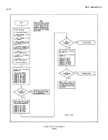
Страница 91: ...TM 11 6625 3071 14 3478A Figure 7 D 6 Flowchart D 7 D 9 ...
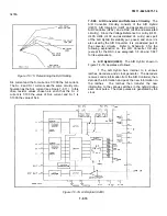
Страница 98: ...TM 11 6625 3071 14 3478A Figure 7 F 2 Simplified Schematic Of The Input Switching Circuitry 7 F 4 ...
Страница 111: ...TM 11 6625 3071 14 Figure 7 F 17 3478A Simplified Reference Circuitry 7 F 16 ...
Страница 122: ...TM 11 6625 3071 14 Table A 2 A 2 HP IB Worksheet A 4 ...
Страница 137: ...TM 11 6625 3071 14 Figure 7 D 2 Flow chart A 7 D 3 ...
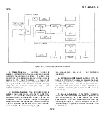
Страница 139: ...TM 11 6625 3071 14 Figure 7 G 2 3478A Block Diagram 7 G 3 ...
Страница 140: ...TM 11 6625 3071 14 Component Locator for Input Circuitry and Ohms Current Source 7 G 4 ...
Страница 141: ...TM 11 6625 3071 14 Figure 7 G 3 Input Circuitry and Ohms Current Source 7 G 5 ...
Страница 142: ...TM 11 6625 3071 14 F G 6 ...
Страница 143: ...TM 11 6625 3071 14 2 Figure 7 G 4 AC to DC Converter 7 G 7 ...
Страница 144: ...TM 11 6625 3071 14 Component Locator for A D Converter and Control Logic 7 G 8 ...
Страница 145: ...TM 11 6625 3071 14 3 Figure 7 G 5 A D Converter and Control Logic 7 G 9 ...
Страница 146: ...TM 11 6625 3071 14 7 G 10 ...
Страница 147: ...TM 11 6625 3071 14 4 Figure 7 G 6 Power Supplies 7 G 11 7 G 12 blank ...
Страница 148: ......
Страница 149: ...PIN NO 057444 ...

