TM 11-6625-3071-14
3478A
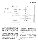
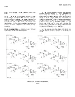
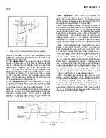
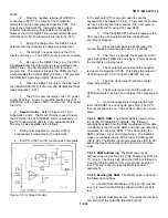
Figure 7-F-7. Simplified A/D Converter
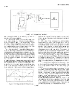
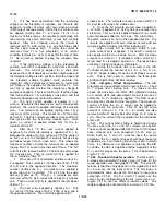
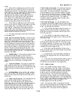
7-F-7 and Figure 7-F-8 for the following simplified ex-
planation of the runup operation.
a.
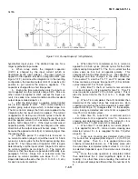
When runup starts, the input voltage (A/D Con-
verter input voltage, not instrument input voltage) is
applied to integrator U401. The resultant input current
(Iin) then charges integrator capacitor C410 and a
certain slope (output of the integrator) is then developed.
This happens at time period TI (see Figure 7-F-8). (The
input voltage is always applied during runup.)
b.
After time period T1, a negative going current is
applied to the integrator for a set time period. This cur-
rent, in addition to the input current, charges C410. This
generates a positive going output slope (the integrator
output). The applied current makes sure that the output
slope that follows will cross zero, whether the input
current is positive or negative. The current is applied for
time period T2.
c. After time period T2, the applied current (not the input
current) is removed and a current of opposite polarity is
then applied to U401 for new time period T3 (T3 is twice
as long as T2). The newly applied current is the same
value as the first applied current (at time T2), but at
opposite polarity. The new current then charges
Figure
Figure 7-F-8. Integrator (U401) Output Slopes
C410 in the opposite direction (C410 is discharged).
This is because the applied current is larger than the in-
put current.
d. When time T3 is completed, the A/D Controller
determines if the output slope crossed zero. If zero
crossing is detected, a current with the same value and
an opposite polarity as the previously applied current is
applied. This current is the same current as the first
applied current and is applied to the integrator for a new
time period T4 (T4 is as long as T3). This current, in
addition to the input current, then charges C410. Since
both currents charge C410, the output slope becomes
steeper and, as shown in Figure 7-F-8, crosses zero.
e.
If no zero crossing (in step c) was detected
(because of a larger input voltage), the same current as
the previously applied current is applied for the new time
period T4. The current is reapplied until zero crossing is
detected. (This is shown as the dashed lines in Figure 7-
F-8).
f. The operation in steps c and d, or in steps c and
e continues until the runup operation is completed. The
total runup operation lasts for 349 ALE ramps (or
counts).
g.
During the runup operation, a counter in the A/D
Controller increments during the positive going slope
periods and decrements during the negative going slope
periods. The counter, in effect, is used to determine the
amount of charge added and subtracted from the input
voltage. From that information, the most significant
digits of the 3478A’s reading is calculated.
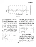
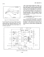
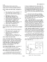
7-F-37. Detailed Explanation of Runup. Figure 7-F-9
illustrates the 3478A runup operation in the 4 1/2 digit
mode. Refer to the figure (and Schematic 3) for the
runup explanation in the following steps. The solid lines
(in the figure) showing the runup sequence is for a
7-F-10
Содержание 3478A
Страница 2: ...TM 11 6625 3071 14 A ...
Страница 4: ...TM 11 6625 3071 14 C D BLANK ...
Страница 12: ...TM 11 6625 3071 14 Table 1 1 Specification 1 2 ...
Страница 13: ...TM 11 6625 3071 14 Table 1 1 Specifications Cont 1 3 ...
Страница 14: ...TM 11 6625 3071 14 Table 1 1 Specifications Cont 1 4 ...
Страница 53: ...TM 11 6625 3071 14 1 ...
Страница 54: ...TM 11 6625 3071 14 2 ...
Страница 55: ...TM 11 6625 3071 14 3 ...
Страница 56: ...TM 11 6625 3071 14 4 ...
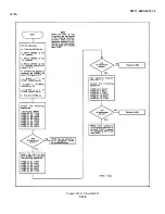
Страница 87: ...TM 11 6625 3071 14 3478A Figure 7 D 3 Flowchart B 7 D 5 ...
Страница 88: ...TM 11 6625 3071 14 3478A Figure 7 D 4 Flowchart C 7 D 6 ...
Страница 91: ...TM 11 6625 3071 14 3478A Figure 7 D 6 Flowchart D 7 D 9 ...
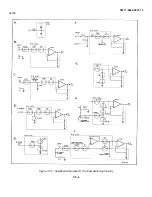
Страница 98: ...TM 11 6625 3071 14 3478A Figure 7 F 2 Simplified Schematic Of The Input Switching Circuitry 7 F 4 ...
Страница 111: ...TM 11 6625 3071 14 Figure 7 F 17 3478A Simplified Reference Circuitry 7 F 16 ...
Страница 122: ...TM 11 6625 3071 14 Table A 2 A 2 HP IB Worksheet A 4 ...
Страница 137: ...TM 11 6625 3071 14 Figure 7 D 2 Flow chart A 7 D 3 ...
Страница 139: ...TM 11 6625 3071 14 Figure 7 G 2 3478A Block Diagram 7 G 3 ...
Страница 140: ...TM 11 6625 3071 14 Component Locator for Input Circuitry and Ohms Current Source 7 G 4 ...
Страница 141: ...TM 11 6625 3071 14 Figure 7 G 3 Input Circuitry and Ohms Current Source 7 G 5 ...
Страница 142: ...TM 11 6625 3071 14 F G 6 ...
Страница 143: ...TM 11 6625 3071 14 2 Figure 7 G 4 AC to DC Converter 7 G 7 ...
Страница 144: ...TM 11 6625 3071 14 Component Locator for A D Converter and Control Logic 7 G 8 ...
Страница 145: ...TM 11 6625 3071 14 3 Figure 7 G 5 A D Converter and Control Logic 7 G 9 ...
Страница 146: ...TM 11 6625 3071 14 7 G 10 ...
Страница 147: ...TM 11 6625 3071 14 4 Figure 7 G 6 Power Supplies 7 G 11 7 G 12 blank ...
Страница 148: ......
Страница 149: ...PIN NO 057444 ...


