TM 11-6625-3071-14
3478A
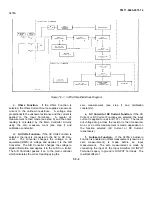
generator which is syncronized by the ALE clock (from
the A/D Controller). The hybrid receives all its control
information from ports P10 through P14 of the A/D
Controller (U462 pins 27 to 31). The information is
transferred over the A, B, C, D, and E lines (U403 pins 5
through 9) of the hybrid.
2.The S-4, S + 4, S-3, S +2, S-l, S + , S-0, and S
+0 currents are developed using resistors RA2 through
RAIO in conjunction with the slope switches.
3.The A/D comparator is also inside the A/D
Hybrid and its input is connected to the output of the A/D
Integrator. The comparator updates its output during
each clock pulse. Since the comparator’s output is
connected to a latch, the out- put is transferred to a TTL
driver during each clock pulse. The TTL driver is a
buffer which connects the output of the latch to the A/D
Con- troller. 4. Dependent on the function selected, the
hybrid connects the DC/Ohms Input Amplifier’s output or
the AC to DC Converter’s output to the A/D Integrator’s
(U401) input resistor (RAI in U403). This is done by the
input switches inside the hybrid.
b. A/D Integrator (U401 and associated circuitry).
The A/D Integrator consists of an amplifier (U401) with
capacitor feedback (C410). Since the amplifier is
inverting, the output slopes of the integrator will be
positive for negative input currents (and vice versa).
c. A/D Controller (U462). The A/D Controller controls
the operation of the A/D Converter. This includes the
control of the runup and rundown operation, and
selecting the correct currents (S-4, S + 4, etc.). Refer to
paragraph 7-F-77 for more information on the A/D
Controller.
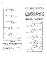
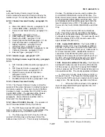
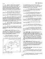
d. Voltage Reference. The Voltage Reference
provides three stable reference voltages: -10 OV, + 10V,
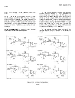
and a buffered -IOV. The circuitry, shown in Figure 7-F-
17, is explained as follows:
1. The -O1V reference voltage is used by the A/D Hybrid
(U403) to develop stable and ac- curate S-4, S + 4, S-3,
etc. currents. The reference voltage is developed by
non-inverting amplifier (U405) using feedback resistors
in U403 and a 7V reference diode (zener diode U461).
The 7V reference diode is connected to the amplifier’s
positive terminal and determines the stabilty of the
reference voltage. The diode voltage is very stable since
the case of the diode has internal heaters to keep the
diode temperature as constant as possible. The
feedback resistors for U405 are in U403 for good
stability.
2. The buffered -IOV is used by the A/D Hybrid as a
stable -10V power supply. The voltage is developed by
X1 gain non-inverting amplifier U404 and the -10V
reference voltage.
3. The + 10V reference voltage is used by the A/D
Hybrid (in conjunction with the -10V reference) to
develop the S-4, S + 4, S-3, etc. currents. The + 10V
reference voltage is also used by the Ohms Current
Source to develop a stable ohms current (see paragraph
7-F-21). The reference voltage is developed using
inverting amplifier U402 and feedback resistors in U403.
7-F-50. 3478A Logic Circuitry
7-F-51. General. The 3478A Logic Circuitry can be
divided into two circuit areas: Chassis Common Cir-
7-F-15
Содержание 3478A
Страница 2: ...TM 11 6625 3071 14 A ...
Страница 4: ...TM 11 6625 3071 14 C D BLANK ...
Страница 12: ...TM 11 6625 3071 14 Table 1 1 Specification 1 2 ...
Страница 13: ...TM 11 6625 3071 14 Table 1 1 Specifications Cont 1 3 ...
Страница 14: ...TM 11 6625 3071 14 Table 1 1 Specifications Cont 1 4 ...
Страница 53: ...TM 11 6625 3071 14 1 ...
Страница 54: ...TM 11 6625 3071 14 2 ...
Страница 55: ...TM 11 6625 3071 14 3 ...
Страница 56: ...TM 11 6625 3071 14 4 ...
Страница 87: ...TM 11 6625 3071 14 3478A Figure 7 D 3 Flowchart B 7 D 5 ...
Страница 88: ...TM 11 6625 3071 14 3478A Figure 7 D 4 Flowchart C 7 D 6 ...
Страница 91: ...TM 11 6625 3071 14 3478A Figure 7 D 6 Flowchart D 7 D 9 ...
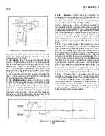
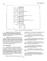
Страница 98: ...TM 11 6625 3071 14 3478A Figure 7 F 2 Simplified Schematic Of The Input Switching Circuitry 7 F 4 ...
Страница 111: ...TM 11 6625 3071 14 Figure 7 F 17 3478A Simplified Reference Circuitry 7 F 16 ...
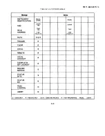
Страница 122: ...TM 11 6625 3071 14 Table A 2 A 2 HP IB Worksheet A 4 ...
Страница 137: ...TM 11 6625 3071 14 Figure 7 D 2 Flow chart A 7 D 3 ...
Страница 139: ...TM 11 6625 3071 14 Figure 7 G 2 3478A Block Diagram 7 G 3 ...
Страница 140: ...TM 11 6625 3071 14 Component Locator for Input Circuitry and Ohms Current Source 7 G 4 ...
Страница 141: ...TM 11 6625 3071 14 Figure 7 G 3 Input Circuitry and Ohms Current Source 7 G 5 ...
Страница 142: ...TM 11 6625 3071 14 F G 6 ...
Страница 143: ...TM 11 6625 3071 14 2 Figure 7 G 4 AC to DC Converter 7 G 7 ...
Страница 144: ...TM 11 6625 3071 14 Component Locator for A D Converter and Control Logic 7 G 8 ...
Страница 145: ...TM 11 6625 3071 14 3 Figure 7 G 5 A D Converter and Control Logic 7 G 9 ...
Страница 146: ...TM 11 6625 3071 14 7 G 10 ...
Страница 147: ...TM 11 6625 3071 14 4 Figure 7 G 6 Power Supplies 7 G 11 7 G 12 blank ...
Страница 148: ......
Страница 149: ...PIN NO 057444 ...

