background image

X90 mobile system

User's manual

Version:

1.20 (January 2019)

Model no.:

MAX90-ENG

Translation of the original manual

All  values  in  this  manual  are  current  as  of  its  publication.  We  reserve  the  right  to  change  the  content  of

this manual without prior notice. B&R Industrial Automation GmbH is not liable for technical/editorial errors or

incomplete information in this manual. In addition, B&R Industrial Automation GmbH shall not be liable for incidental

or consequential damages in connection with or arising from the furnishing, performance or use of this material.

The software names, hardware names and trademarks used in this document are registered by their respective

companies.

Содержание X90

Страница 1: ...t prior notice B R Industrial Automation GmbH is not liable for technical editorial errors or incomplete information in this manual In addition B R Industrial Automation GmbH shall not be liable for i...

Страница 2: ...t 11 2 4 1 Assemble connect ready 11 2 5 Sophisticated mechanics 12 2 6 Diagnostics 12 2 7 Embedded parameter chip 13 2 8 Multifunction inputs and outputs 13 2 9 Space for options 13 2 10 Flexibility...

Страница 3: ...2 2 3 Technical data 87 5 2 2 4 LED status indicators 91 5 2 2 5 Operating and connection elements 95 5 2 2 6 Block diagram 102 5 2 2 7 Switching inductive loads MF DO 108 5 2 2 8 Derating 109 5 2 2 9...

Страница 4: ...scription 326 6 Accessories 337 6 1 Overview 337 6 2 Bus controller modules 338 6 2 1 X67HB8880 L12 338 6 2 1 1 Order data 338 6 2 1 2 Technical data 339 6 3 Installation tool 340 6 3 1 X67ACTQMX 340...

Страница 5: ...7 3 Vehicle requirements 358 7 3 1 Requirements for immunity to disturbances 358 7 3 2 Emission requirements 360 7 3 3 Mechanical conditions 361 7 4 Requirements for industry 362 7 4 1 Requirements fo...

Страница 6: ...Slot PLC e g B R LS251 or comparable product relevant safety precautions e g the provision of safety devices such as emergency switch off etc must be ob served in accordance with applicable national a...

Страница 7: ...ment Individual components ESD protective measures for individual components are implemented throughout B R conductive floors shoes wrist straps etc The increased ESD protective measures for individua...

Страница 8: ...necessary to separate out the different materials so that devices can undergo an environmentally friendly recycling process Component Disposal X90 mobile modules Cables Electronics recycling Cardboar...

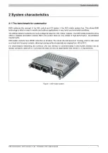
Страница 9: ...d on X90 mobile modules The X90 mobile product line thus offers a scalable automation solution that is the perfect basis for very simple to high performance decentralized requirements X90 mobile produ...

Страница 10: ...me communication Although most requirements are covered by the standard equipment of the CPUs there are up to four multipurpose slots for additional interface modules 2 2 2 B R Automation Studio B R A...

Страница 11: ...t for manual wiring to a minimum 2 4 1 Assemble connect ready The four mounting points allow the X90 mobile system to be installed quickly and easily using the screws The customer can screw the device...

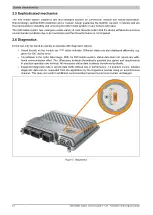
Страница 12: ...Diagnostics Errors can only be found as quickly as possible with diagnostic options Visual directly on the module via LED status indicator Different states are also displayed differently e g green fo...

Страница 13: ...ignal without changing the control system Multifunction PWM outputs MF PWM Power outputs up to 6 A PWM frequency configurable up to 1 kHz High side and low side outputs Current measurement 10 A Can be...

Страница 14: ...p to 4 A per output Parallel connection of outputs Diagnostics capable Special purpose modules Interface modules Special purpose sensors Hydrostatic control Mixed modules Condition monitoring 2 10 Fle...

Страница 15: ...and ingress of foreign bodies and water First number 6 Complete protection against contact protection against ingress of dust Second number 9K Water vapor is not permitted to penetrate in harmful quan...

Страница 16: ...1 X90xx17xxxx mobile System Dimensions 250 mm 231 mm 43 5 mm 212 mm 215 mm 217 mm 6 5 11 5 Figure 4 X90xx17xxxx Dimensions 3 2 Design support 3 2 1 CAD support The dimensions are in 2D with the ECAD...

Страница 17: ...ile machine the ground connections must be provided via a suitable ground rail We recommend providing the ground connections as close as possible to the X90 mobile device to ensure short connection li...

Страница 18: ...ile system with the connection facing upwards This could lead to permanent stress on the single core seals due to standing water ice or chemicals To ensure sufficient air circulation a specified clear...

Страница 19: ...1 20 Translation of the original manual 19 Vertical installation This is the recommended mounting orientation In a horizontal mounting orientation the orientation can be selected as required Standing...

Страница 20: ...ion 20 X90 mobile system User s manual V 1 20 Translation of the original manual 3 6 X90xx17xxxx Installation with connector 80 mm 316 mm 296 mm 311 mm 267 mm 287 mm 56 mm 85 mm 36 mm 65 mm Figure 6 I...

Страница 21: ...ive covers are included in delivery The torque for the wire caps is 0 6 Nm Information When using third party connectors it is strongly recommended to ensure that the contacts are gold Au coated B R c...

Страница 22: ...r device groups Failure to follow the safety notices covered in this manual Malfunctions caused by the external safety relay 3 9 2 Qualified personnel The safety function must be implemented by person...

Страница 23: ...hat combines maximum flexibility with optimum component density Robust die cast aluminum housing Passive cooling Fast startup times Resistant to shock and vibration Modular construction Optimal EMC pr...

Страница 24: ...depending on the variant TechGuard 0TG 220198 xxx 00 With the pressure equalization membrane made of polytetrafluoroethylene Teflon which prevents the ingress of water but allows the diffusion of vap...

Страница 25: ...lling Removing the X90 mobile system The X90 mobile system is secured with four M6 screws to the smoothest possible surface in the holes provided for this purpose with a torque suitable for the select...

Страница 26: ...2 2 Figure 10 Unused pins Blind plugs image by Molex Important Unused pins must be fitted with blind plugs otherwise the IP rating cannot be guaranteed Mating connector X1 is unlocked by pulling out t...

Страница 27: ...ting the cable image by Molex Lock mating connector X1 again by pushing the gray latch back into mating connector X1 Figure 15 Locking mating connector X1 Information If the gray latch jams when tryin...

Страница 28: ...p 90 until the latch locks onto the wire cap Lock Figure 17 Rotating the latch Figure 18 Locking the latch The stranded wire must be protected against vibration using a cable tie through the clap on t...

Страница 29: ...tening clip Figure 21 Rotating the latch To remove the wire cap from mating connector X1 the two locking points must be disengaged with a screwdriver This is done by pressing the screwdriver into one...

Страница 30: ...anual V 1 20 Translation of the original manual Press the cable into mating connector X1 1 Insert the removal tool into the correct slots 2 Remove the cable 3 Removal tool 0 6 mm Removal tool 1 5 mm 1...

Страница 31: ...Ethernet 10 100BASE T on M12 3 CAN on CMC connector 24 multifunction I O channels 2 sensor power supply 4 option board slots die cast alu minum housing service access window LED status indicators 35 X...

Страница 32: ...1 2 2 X90 option boards Digital inputs Model number Short description Page X90DI110 10 00 X90 mobile option board DI 10 digital inputs 9 to 32 VDC optional sink source optional counter input 50 kHz c...

Страница 33: ...MF PWM 8 16 X X X MF DO 4 8 X X MF AI 8 16 X X MF DI 4 8 X X X90AO410 0x 00 Output Input Multifunction I O Quantity PWM Digital Analog PWM signal Temperature Analog Counter functionality Digital MF A...

Страница 34: ...tem is a controller with a powerful ARM processor and up to 48 multifunction I O channels Basic features include interfaces for CAN USB and Ethernet The extremely robust die cast aluminum housing prov...

Страница 35: ...ital inputs 9 to 32 VDC op tional sink source optional counter input 50 kHz configuration using software Digital outputs X90PO210 08 00 X90 mobile option board PWM 8x PWM outputs 9 to 32 VDC max 4 A w...

Страница 36: ...rload MF DO and MF PWM Yes Overtemperature Yes using software and status LED CPU redundancy possible No ACOPOS support Yes reACTION capable I O channels No Visual Components support Yes Overvoltage pr...

Страница 37: ...ut with 50 kHz counter frequency gate measurement Multifunction analog inputs MF AI Quantity 8 16 Functions Universal analog input 12 bit digital converter resolution integrated in put protection digi...

Страница 38: ...polarity protection Yes Input filter 1st order low pass cutoff frequency of voltage input 350 Hz current input 200 Hz Max error at 25 C Voltage Gain 1 4 Offset 1 5 Current Gain 1 4 Offset 1 6 Max gai...

Страница 39: ...cutoff if overcurrent or short circuit occurs integrated protection for switching inductances Design FET positive negative switching channels can be connected in parallel 9 Diagnostic status Output mo...

Страница 40: ...sed 9 For additional information about parallel connections see chapter Derating 10 Sum of MF DO MF PWM 11 Applied only if mating connector M12 CPC connected or with M12 protective covers 0 6 Nm torqu...

Страница 41: ...error code consists of 4 switch on phases with short 150 ms or long 600 ms duration The error code is repeated every 2 seconds All times in ms RAM error Hardware error 150 150 150 300 300 300 600 200...

Страница 42: ...service access window again connect it to the X90 mobile system again and turn it clockwise with a coin until the markings on the cover point to the markings on the housing The button must be pressed...

Страница 43: ...ode see Reset button on page 42 or an invalid flash drive 2 Establish a physical online connection between the programming device PC or industrial PC and CPU e g over an Ethernet network 3 Before you...

Страница 44: ...3 Tx Transmit data 4 Rx Receive data 5 2 1 5 7 USB interface USB 1 Interface IF4 is a non electrically isolated USB interface The connection is made via a USB interface 1 1 2 0 The USB interface can...

Страница 45: ...upply 2 Mainboard 5 V E2 Sensor power supply 1 Mainboard 5 V 10 V F2 MF DI Mainboard 2 G2 MF DI Mainboard 4 H2 MF AI Mainboard 5 J2 MF AI Mainboard 7 K2 Ignition Mainboard KL15 L2 GND M2 MF PWM 6 A Ma...

Страница 46: ...ainboard 15 F4 Function Option board 1 2 G4 MF PWM 6 A Mainboard 13 H4 Function Vcc GND Option board 2 10 CMC header X1 C Black Pinout Pin Name Slot Channel A1 Function Option board 2 6 B1 Function Op...

Страница 47: ...signal is interrupted then the power supply for the power outputs is cut off 5 2 1 5 8 4 Ignition plus The switched plus is the plus pole coupled to the ignition lock and also referred to as terminal...

Страница 48: ...31 0 V GND Relay active MF DO high side MF PWM push pull Option board 1 Option board 2 Option board 3 Option board 4 CPU Power supply Reset controller A D converter Sensor SensorSv Sensor power suppl...

Страница 49: ...onfiguration 6 9 10 22 k Digital input 12 24 V ECU GND KL30 5 A slow blow Multifunction analog input MF AI diagnostics capable voltage input A D converter Analog input 12 24 V ECU GND KL30 5 A slow bl...

Страница 50: ...nput ECU Analog GND 6 9 24 9 k Voltage source 0 to 10 32 V Multifunction analog input MF AI current input A D converter Analog input ECU Analog GND Current source 0 to 20 mA PTC Shunt Multifunction ou...

Страница 51: ...k Digital input GND Status Status Current Relay active Sink configuration ECU Vcc Supply voltage Vs1 10 A slow blow Digital output Sensor power supply permanently on Digital input Sensor input positiv...

Страница 52: ...Sensor input positive switching Note that in the event of power failure or if the enable relay is cut off then the power supply for the sensor is also cut off This is because the module is supplied w...

Страница 53: ...active PWM GND ECU Vcc Supply voltage Vs1 10 A slow blow Multifunction output MF PWM PWM output sink circuit 12 24 V output power supply Digital output 10 k PWM GND Status Current Status Current Digi...

Страница 54: ...itching cycles second at 90 duty cycle Coil inductance 32 V 9 V 1 H 1 output per IC simultaneous switching All outputs simultaneous switching Important The maximum permissible inductive loads accordin...

Страница 55: ...mple 1 Parallel connection of 2 outputs with inductive load 6 A Load per channel 6 A 2 3 A Permissible switching frequency 1500 3 A 500 Hz Example 2 Parallel connection of 2 outputs with inductive loa...

Страница 56: ...tage dip of 1 ms The X90 mobile system is not affected by this This can have a negative influence on other components using the same power supply however Power supply of other devices ECU Vcc Ipk Buff...

Страница 57: ...and outputs Information All values in the register description correspond to the maximum hardware variant Gaps in the regis ters result from smaller hardware variants X90CP17x 24 00 X90CP17x 48 00 1...

Страница 58: ...talInput17 Bit 0 1095 ShortCircuitDigitalInput24 Bit 7 Communication State of the digital inputs Open circuit Status of the digital inputs USINT WirebreakDigitalInput09 Bit 0 1097 WirebreakDigitalInpu...

Страница 59: ...0 1101 UnderflowAnalogInput16 Bit 7 Status of the analog inputs USINT UnderflowAnalogInput17 Bit 0 1103 UnderflowAnalogInput24 Bit 7 Communication Overflow of analog inputs Status of the analog input...

Страница 60: ...ErrorDigitalOutput48 Bit 7 Communication Overload of the digital outputs Overload cutoff USINT OverloadDigitalOutput25 Bit 0 2059 OverloadDigitalOutput32 Bit 7 Overload cutoff USINT OverloadDigitalOut...

Страница 61: ...current monitoring USINT CurrentOverloadShutdown Bit 2 StatusSensorSupply Bit 3 OutputEnabled Bit 4 4097 StatusIgnition Bit 5 20481 CurrentOverloadShutdownClear Bit 2 Communication Measuring module cu...

Страница 62: ...gDigitalFilterN index N 33 to 48 USINT Configuration Edge detection Selection of master edge 32833 N 1 2 cfgEdgeDetectMasterUnit0N index N 1 to 8 USINT Configuration Edge detection Mode settings 32817...

Страница 63: ...measurement diagnostics 60 Digital input source 6 5 k pull up with adjustable switching threshold 61 Digital input source 9 k pull up with adjustable switching threshold 62 Digital input source 18 k p...

Страница 64: ...designed for sink and source circuits Topics in this section Filter time Threshold value Hysteresis Input values of the digital inputs Not all options are available for an input The threshold value a...

Страница 65: ...configured as a digital input the hysteresis mV can be set with this register in order to avoid fre quent state changes in the measurement range near the threshold value When taking into account the...

Страница 66: ...tion Digital input with voltage measurement diagnostics or Digital input with current measurement diagnostics The resistors are connected in series or parallel to the sensor The following values are d...

Страница 67: ...n Value Information 0 No open circuit 0 WirebreakDigitalInput17 1 Open circuit 0 No open circuit 7 WirebreakDigitalInput24 1 Open circuit Bit structure Bit Description Value Information 0 No short cir...

Страница 68: ...of the basic function for either just the master edge or both master and slave edges Data type Values Information 0x00 Disabled 0x80 Reaction to master edge USINT 0xC0 Reaction to master slave edge 5...

Страница 69: ...edge on channel 2 14 Rising edge on channel 8 15 Falling edge on channel 8 USINT 255 Disabled 5 2 1 12 6 5 Edge detection Timestamp Name MasterTime01 to MasterTime08 SlaveTime01 to SlaveTime08 The exa...

Страница 70: ...cfgCounterModeUnit01 or channel 5 cfg CounterModeUnit03 then the following channel cfgCounterModeUnit02 or cfgCounterModeUnit04 can no longer be used Chan nel Event counter AB incremental counter DF...

Страница 71: ...the counter value 1 CounterReset02 1 Reset the counter 0 Do not clear the counter value 2 CounterReset03 1 Reset the counter 0 Do not clear the counter value 3 CounterReset04 1 Reset the counter 0 Di...

Страница 72: ...high level 1 Enabled 0 Disabled 4 Counter 01 Input 01 low level 1 Enabled 0 Disabled 5 Counter 01 Input 02 low level 1 Enabled 0 Disabled 6 Counter 01 Input 03 low level 1 Enabled 0 Disabled 7 Counte...

Страница 73: ...limitation if this is performed Data type Values USINT See the bit structure Bit structure Bit Description Value Information 0 Disabled default 1 Filter level 2 2 Filter level 4 3 Filter level 8 4 Fi...

Страница 74: ...em tick Input jump 1 2 3 4 5 6 7 8 Input value Internally tracked input value before the filter Figure 25 Adjusted input value for input jump Example 2 A disturbance interferes with the input value Th...

Страница 75: ...h the following settings Input ramp limiting 0 Filter level 2 or 4 0 8000 16000 160 s Input jump 1 2 3 4 5 6 7 8 Input value Calculated value Filter level 2 Calculated value Filter level 4 Figure 27 C...

Страница 76: ...logInput24 OverflowAnalogInput09 to OverflowAnalogInput16 OverflowAnalogInput17 to OverflowAnalogInput24 OutOfRangeAnalogInput09 to OutOfRangeAnalogInput16 OutOfRangeAnalogInput17 to OutOfRangeAnalogI...

Страница 77: ...ese registers Note The digital output can only be switched if it is configured as the main output Parallel outputs are switched with the corresponding main output Data type Values USINT See the bit st...

Страница 78: ...icated in these registers If the switched output level of a digital output does not correspond to the read back value then the corresponding bit is set As soon as the switched output level again corre...

Страница 79: ...then the corresponding bit is not maintained Data type Values USINT See the bit structure Bit structure Bit Description Value Information 0 Not cut off 0 OverloadDigitalOutput25 1 Cutoff due to overl...

Страница 80: ...Output48 will not be reset until after the minimum cutoff duration 5 sec has elapsed Data type Values USINT See the bit structure Bit structure Bit Description Value Information 0 No acknowledgment 0...

Страница 81: ...eriod48 These registers define the period duration i e the time base for the respective PWM output This time represents the 100 value which can be incremented in 0 1 steps through the duty cycle Data...

Страница 82: ...bit 1 LSB of the INT value corresponds to 610 A Data type Values Information INT 32768 to 32767 Measured current Name Current33 to Current48 These registers contain the analog current measured value...

Страница 83: ...0 2 CurrentOverloadShutdownClear 1 Rising edge Digital outputs are re enabled after summation current monitor ing is disabled 0 Outputs disabled 3 OutputEnable 1 Outputs enabled 4 to 7 Reserved 5 2 1...

Страница 84: ...r power supply Name cfgOpMgmt_Mode Data type Values USINT See the bit structure Bit structure Bit Description Value Information 0 5 V sensor power supply 0 Voltage selection of sensor power supply 1 1...

Страница 85: ...rful ARM processor and up to 48 multifunction I O channels Basic features include connections for CAN USB Ethernet and the real time POWERLINK bus system The extremely robust die cast aluminum housing...

Страница 86: ...ts Digital inputs X90DI110 10 00 X90 mobile option board DI 10 digital inputs 9 to 32 VDC op tional sink source optional counter input 50 kHz configuration using software Digital outputs X90PO210 08 0...

Страница 87: ...wer supply when output Low Yes Load break MF DO and MF PWM Load break switched on Per application POWERLINK Yes using status LED Analog inputs Voltage Ue 0 5 V applicative Current Ie 1 mA applicative...

Страница 88: ...controlled node Type Type 4 4 Design M12 D keyed Cable length Max 100 m between two stations segment length Transfer rate 100 Mbit s Transfer Physical layer 100BASE TX Half duplex Yes Full duplex No A...

Страница 89: ...voltage 9 to 32 VDC Input current at 24 VDC MF DI Typ 1 2 2 5 3 6 mA configurable MF AI Typ 1 2 2 5 3 6 mA configurable MF DO Typ 2 5 mA MF PWM Typ 2 5 mA Input filter Hardware MF DI 3 s if switching...

Страница 90: ...WM 50 m Residual voltage 1 V at 4 A nominal current Peak short circuit current MF DO 90 A MF PWM 50 A Switching frequency Resistive load MF DO Max 250 Hz Inductive load MF DO Load current 4 A Max 4 mH...

Страница 91: ...nnected externally 3 Can be set in Automation Studio 4 See Automation Help under Communication POWERLINK General information Hardware IF LS for more information 5 Based on the current measured value 6...

Страница 92: ...e interface is operated as an Ethernet interface Table LED S E Interface in Ethernet mode 5 2 2 4 1 2 POWERLINK V2 mode Error message LED S E Green Red Description Off On The interface is in the error...

Страница 93: ...n this mode Cyclic communication is not yet taking place Controlled node CN The CN can be configured by the MN in this mode The CN waits until it receives an SoC frame and then switches to mode PRE_OP...

Страница 94: ...orrect configuration or defective hardware The error code is indicated by LED S E blinking red The blinking signal of the error code consists of 4 switch on phases with short 150 ms or long 600 ms dur...

Страница 95: ...mobile modules X90 mobile system User s manual V 1 20 Translation of the original manual 95 5 2 2 5 Operating and connection elements IF2 Ethernet IF3 POWERLINK IF4 USB 2 I O I O IF7 to IF9 CAN bus I...

Страница 96: ...service access window again connect it to the X90 mobile system again and turn it clockwise with a coin until the markings on the cover point to the markings on the housing The button must be pressed...

Страница 97: ...ode see Reset button on page 96 or an invalid flash drive 2 Establish a physical online connection between the programming device PC or industrial PC and CPU e g over an Ethernet network 3 Before you...

Страница 98: ...Pinout Interface Pin Name Assignment 1 Tx Transmit data 2 Rx Receive data 3 Tx Transmit data 4 Rx Receive data 5 2 2 5 8 USB interface USB 1 Interface IF4 is a non electrically isolated USB interface...

Страница 99: ...upply 2 Mainboard 5 V E2 Sensor power supply 1 Mainboard 5 V 10 V F2 MF DI Mainboard 2 G2 MF DI Mainboard 4 H2 MF AI Mainboard 5 J2 MF AI Mainboard 7 K2 Ignition Mainboard KL15 L2 GND M2 MF PWM 6 A Ma...

Страница 100: ...ainboard 15 F4 Function Option board 1 2 G4 MF PWM 6 A Mainboard 13 H4 Function Vcc GND Option board 2 10 CMC header X1 C Black Pinout Pin Name Slot Channel A1 Function Option board 2 6 B1 Function Op...

Страница 101: ...e signal is interrupted then the power supply for the power outputs is cut off 5 2 2 5 9 4 Ignition plus The switched plus is the plus pole coupled to the ignition lock and also referred to as termina...

Страница 102: ...0 V GND Relay active MF DO high side MF PWM push pull Option board 1 Option board 2 Option board 3 Option board 4 CPU Power supply Reset controller A D converter Sensor SensorSv 5 10 V Sensor power su...

Страница 103: ...configuration 6 9 10 22 k Digital input 12 24 V ECU GND KL30 5 A slow blow Multifunction analog input MF AI diagnostics capable voltage input A D converter Analog input 12 24 V ECU GND KL30 5 A slow b...

Страница 104: ...nput ECU Analog GND 6 9 24 9 k Voltage source 0 to 10 32 V Multifunction analog input MF AI current input A D converter Analog input ECU Analog GND Current source 0 to 20 mA PTC Shunt Multifunction ou...

Страница 105: ...k Digital input GND Status Status Current Relay active Sink configuration ECU Vcc Supply voltage Vs1 10 A slow blow Digital output Sensor power supply permanently on Digital input Sensor input positiv...

Страница 106: ...t Sensor input positive switching Note that in the event of power failure or if the enable relay is cut off then the power supply for the sensor is also cut off This is because the module is supplied...

Страница 107: ...active PWM GND ECU Vcc Supply voltage Vs1 10 A slow blow Multifunction output MF PWM PWM output sink circuit 12 24 V output power supply Digital output 10 k PWM GND Status Current Status Current Digi...

Страница 108: ...witching cycles second at 90 duty cycle Coil inductance 32 V 9 V 1 H 1 output per IC simultaneous switching All outputs simultaneous switching Important The maximum permissible inductive loads accordi...

Страница 109: ...ample 1 Parallel connection of 2 outputs with inductive load 6 A Load per channel 6 A 2 3 A Permissible switching frequency 1500 3 A 500 Hz Example 2 Parallel connection of 2 outputs with inductive lo...

Страница 110: ...tage dip of 1 ms The X90 mobile system is not affected by this This can have a negative influence on other components using the same power supply however Power supply of other devices ECU Vcc Ipk Buff...

Страница 111: ...and outputs Information All values in the register description correspond to the maximum hardware variant Gaps in the regis ters result from smaller hardware variants X90CP17x 24 00 X90CP17x 48 00 1...

Страница 112: ...talInput17 Bit 0 1095 ShortCircuitDigitalInput24 Bit 7 Communication State of the digital inputs Open circuit Status of the digital inputs USINT WirebreakDigitalInput09 Bit 0 1097 WirebreakDigitalInpu...

Страница 113: ...0 1101 UnderflowAnalogInput16 Bit 7 Status of the analog inputs USINT UnderflowAnalogInput17 Bit 0 1103 UnderflowAnalogInput24 Bit 7 Communication Overflow of analog inputs Status of the analog input...

Страница 114: ...ErrorDigitalOutput48 Bit 7 Communication Overload of the digital outputs Overload cutoff USINT OverloadDigitalOutput25 Bit 0 2059 OverloadDigitalOutput32 Bit 7 Overload cutoff USINT OverloadDigitalOu...

Страница 115: ...current monitoring USINT CurrentOverloadShutdown Bit 2 StatusSensorSupply Bit 3 OutputEnabled Bit 4 4097 StatusIgnition Bit 5 20481 CurrentOverloadShutdownClear Bit 2 Communication Measuring module cu...

Страница 116: ...gDigitalFilterN index N 33 to 48 USINT Configuration Edge detection Selection of master edge 32833 N 1 2 cfgEdgeDetectMasterUnit0N index N 1 to 8 USINT Configuration Edge detection Mode settings 32817...

Страница 117: ...measurement diagnostics 60 Digital input source 6 5 k pull up with adjustable switching threshold 61 Digital input source 9 k pull up with adjustable switching threshold 62 Digital input source 18 k p...

Страница 118: ...designed for sink and source circuits Topics in this section Filter time Threshold value Hysteresis Input values of the digital inputs Not all options are available for an input The threshold value a...

Страница 119: ...s configured as a digital input the hysteresis mV can be set with this register in order to avoid fre quent state changes in the measurement range near the threshold value When taking into account the...

Страница 120: ...ation Digital input with voltage measurement diagnostics or Digital input with current measurement diagnostics The resistors are connected in series or parallel to the sensor The following values are...

Страница 121: ...on Value Information 0 No open circuit 0 WirebreakDigitalInput17 1 Open circuit 0 No open circuit 7 WirebreakDigitalInput24 1 Open circuit Bit structure Bit Description Value Information 0 No short ci...

Страница 122: ...e of the basic function for either just the master edge or both master and slave edges Data type Values Information 0x00 Disabled 0x80 Reaction to master edge USINT 0xC0 Reaction to master slave edge...

Страница 123: ...edge on channel 2 14 Rising edge on channel 8 15 Falling edge on channel 8 USINT 255 Disabled 5 2 2 12 6 5 Edge detection Timestamp Name MasterTime01 to MasterTime08 SlaveTime01 to SlaveTime08 The exa...

Страница 124: ...1 cfgCounterModeUnit01 or channel 5 cfg CounterModeUnit03 then the following channel cfgCounterModeUnit02 or cfgCounterModeUnit04 can no longer be used Chan nel Event counter AB incremental counter DF...

Страница 125: ...the counter value 1 CounterReset02 1 Reset the counter 0 Do not clear the counter value 2 CounterReset03 1 Reset the counter 0 Do not clear the counter value 3 CounterReset04 1 Reset the counter 0 Di...

Страница 126: ...high level 1 Enabled 0 Disabled 4 Counter 01 Input 01 low level 1 Enabled 0 Disabled 5 Counter 01 Input 02 low level 1 Enabled 0 Disabled 6 Counter 01 Input 03 low level 1 Enabled 0 Disabled 7 Counte...

Страница 127: ...limitation if this is performed Data type Values USINT See the bit structure Bit structure Bit Description Value Information 0 Disabled default 1 Filter level 2 2 Filter level 4 3 Filter level 8 4 Fi...

Страница 128: ...em tick Input jump 1 2 3 4 5 6 7 8 Input value Internally tracked input value before the filter Figure 31 Adjusted input value for input jump Example 2 A disturbance interferes with the input value Th...

Страница 129: ...th the following settings Input ramp limiting 0 Filter level 2 or 4 0 8000 16000 160 s Input jump 1 2 3 4 5 6 7 8 Input value Calculated value Filter level 2 Calculated value Filter level 4 Figure 33...

Страница 130: ...logInput24 OverflowAnalogInput09 to OverflowAnalogInput16 OverflowAnalogInput17 to OverflowAnalogInput24 OutOfRangeAnalogInput09 to OutOfRangeAnalogInput16 OutOfRangeAnalogInput17 to OutOfRangeAnalogI...

Страница 131: ...ese registers Note The digital output can only be switched if it is configured as the main output Parallel outputs are switched with the corresponding main output Data type Values USINT See the bit st...

Страница 132: ...dicated in these registers If the switched output level of a digital output does not correspond to the read back value then the corresponding bit is set As soon as the switched output level again corr...

Страница 133: ...I then the corresponding bit is not maintained Data type Values USINT See the bit structure Bit structure Bit Description Value Information 0 Not cut off 0 OverloadDigitalOutput25 1 Cutoff due to over...

Страница 134: ...Output48 will not be reset until after the minimum cutoff duration 5 sec has elapsed Data type Values USINT See the bit structure Bit structure Bit Description Value Information 0 No acknowledgment 0...

Страница 135: ...eriod48 These registers define the period duration i e the time base for the respective PWM output This time represents the 100 value which can be incremented in 0 1 steps through the duty cycle Data...

Страница 136: ...bit 1 LSB of the INT value corresponds to 610 A Data type Values Information INT 32768 to 32767 Measured current Name Current33 to Current48 These registers contain the analog current measured value...

Страница 137: ...d 0 2 CurrentOverloadShutdownClear 1 Rising edge Digital outputs are re enabled after summation current monitor ing is disabled 0 Outputs disabled 3 OutputEnable 1 Outputs enabled 4 to 7 Reserved 5 2...

Страница 138: ...r power supply Name cfgOpMgmt_Mode Data type Values USINT See the bit structure Bit structure Bit Description Value Information 0 5 V sensor power supply 0 Voltage selection of sensor power supply 1 1...

Страница 139: ...tage output Communication to the mainboard is implemented using X2X Link The pins in use can also be used as digital inputs it is possible to toggle them between sink mode and source mode 9 to 32 VDC...

Страница 140: ...gurable Input delay 0 5 ms at 160 s sampling rate Switching threshold 50 supply voltage Analog outputs Quantity 0 to 4 depends on the use of multifunction inputs outputs 0 to 8 depends on the use of m...

Страница 141: ...hanical properties Dimensions Width 47 mm Length 95 mm Table 18 X90AO410 04 00 X90AO410 08 00 Technical data 1 Based on the entire output range 2 Based on the current output value 3 Depends on the mai...

Страница 142: ...6 9 10 22 k Supply voltage Vb2 Digital input KL30 12 24 V ECU Sensor input negative switching GND 5 A slow blow Digital input positive switching A D converter or Comparator Sink configuration 6 9 10 2...

Страница 143: ...X90 mobile modules X90 mobile system User s manual V 1 20 Translation of the original manual 143 Analog current output Analog output ECU Analog GND 500 Current source 0 2 to 20 mA Analog GND...

Страница 144: ...the output channels on off USINT OutputEnable01 Bit 0 2 OutputEnable08 Bit 7 Communication Output values of the analog outputs 6 N 1 4 AnalogOutput0N index N 1 to 8 INT Configuration Digital input fil...

Страница 145: ...or all digital inputs The filter value can be configured in steps of 100 s Data type Values USINT See the bit structure Bit structure Data type Values Information 0 No software filter 1 0 1 ms 10 1 ms...

Страница 146: ...transferred the module outputs the corresponding current or voltage Data type Values Information INT 0 to 32767 Current or voltage value 0 to 10 V or 0 to 20 mA Note The analog output can only be cont...

Страница 147: ...he time and frequency domain also allows measurements to be evaluated externally or archived 4 channel vibration measurement and analysis module 24 bit resolution at 51 562 kHz IEPE power supply Exten...

Страница 148: ...greater for more than 1 ms Input voltage range Common mode voltage UCM 1 to 17 V Differential voltage UD UCM 7 V 10 V UCM 7 V 17 V UCM Conversion procedure Sigma delta Crosstalk between channels 70 dB...

Страница 149: ...4 Shielding The following points for shielding the sensor lines must be observed The shield of the sensor lines must be applied over a large area and with low impedance in the area of the CMC header...

Страница 150: ...der The signals of X90CM480 option boards with frequency components up to 10 kHz are no problem here 5 4 1 3 6 Gain curve The following diagram shows a typical gain curve for the module 60 50 40 30 20...

Страница 151: ...general information such as serial number system time and heat sink temperature This module contains the following general data points FirmwareVersion HardwareVariant ModuleID SerialNumber General da...

Страница 152: ...4 REAL SensitivitySensor0N index N 1 to 4 REAL Vdi3832KtHighFrequency0N index N 1 to 4 REAL Vdi3832KtRaw0N index N 1 to 4 REAL Characteristic values transferred in Flatstream CrestFactorRaw0N index N...

Страница 153: ...dMaxN index N 01 to 32 UDINT 3076 N 8 FrequencyBandMinN index N 01 to 32 UDINT 506 N 24 FrequencyBandNConfig index N 01 to 32 UINT 1194 N 24 FrequencyBandNConfigRead index N 01 to 32 UINT 514 N 24 Fre...

Страница 154: ...le high pass filter for the whole module that can be configured using register HighFrequen cyConfig on page 185 Possible settings are 500 Hz 1 kHz and 2 kHz This high pass affects all high frequency a...

Страница 155: ...measured with the highest possible accuracy This adjustment is made in multiple steps Each step amplifies the input signal more than the last If the signal was very small for a long time and a impact...

Страница 156: ...351 in 1 Hz 1 The driver reduces larger values to 655 35 5 4 1 5 4 2 AutogainDelay Name AutogainDelay01 This register can be used to configure the autogain delay for all 4 channels To ensure that even...

Страница 157: ...Before a buffer can be uploaded all the data it contains must be locked The characteristic values associated with the locked buffers are transferred in the Flatstream characteristic values as soon as...

Страница 158: ...nel 4 EnableVelocityCalculation 1 Calculation enabled 12 13 Reserved 0 0 8192 measured values 14 Buffer length 1 65535 measured values 15 Reserved 1 EnableVelocityCalculation This bit can be used to e...

Страница 159: ...ked 4 BufferLockValid01 or DataLockValid011 1 Data locked consistent and valid 0 No error 5 Channel 1 Overflow01 1 Overflow of one or more characteristic values 0 No error 8 Channel 4 Overflow04 1 Ove...

Страница 160: ...ed on the bus Here the direct input signal raw signal max 10 kHz with a sampling frequency of 25 781 kHz is always used and is not mean adjusted The value is scaled according to the configuration See...

Страница 161: ...e ignored during an ongoing measurement The runtime on the bus can cause retrig gering before the toggle bit has changed If a shorter sample time than the X2X Link cycle time is configured the last co...

Страница 162: ...gInput04 x For possible values see bits 0 1 0 Continuous with enable 8 Trigger mode of AnalogInput01 1 Once with trigger 0 Continuous with enable 11 Trigger mode of AnalogInput04 1 Once with trigger 0...

Страница 163: ...haracteristic value configured in AnalogInputConfig on page 162 for the respective channel is calculated The number of samples configured in SamplesAnalogInput on page 165 is used The calculated value...

Страница 164: ...Information The configured scaling value is always based on a 100 mV g sensor Any sensor that has a different sensor sensitivity must be reflected in the configuration Data type Values UINT See the b...

Страница 165: ...lically in register AnalogInputSamples on page 163 is used and displayed in the associated analog input with the configured scaling Data type Values UINT See the bit structure Bit structure Bit Explan...

Страница 166: ...splayed in mg or mm s or as non dimensional values kurtosis crest factor skewness and Vdi3832 depending on the characteristic value Additional characteristic values In addition to the characteristic v...

Страница 167: ...t for each characteristic value of the respective channel Data type Values UINT See the bit structure Bit structure Bit Description Value Information 0 No error 0 PeakHighFrequency 1 Overflow 0 No err...

Страница 168: ...ivity 5 4 1 5 6 7 PeakHighFrequencyRefCalculated Name PeakHighFrequencyRefCalculated01 to PeakHighFrequencyRefCalculated04 Reference value correct state used by the module for the absolute maximum of...

Страница 169: ...lue correct state specified by the application for the RMS value of the raw signal used to calculate Vdi3832 K t of the raw signal Data type Information REAL Range of values depends on sensor sensitiv...

Страница 170: ...the input signal up to the configured maximum frequency KurtosisRaw Kurtosis fourth statistical moment of the input signal up to the configured maximum frequency Vdi3832KtRaw Relationship of the refe...

Страница 171: ...egisters for reading the absolute maximum of the high pass filtered input signal of the respective channel PeakHighFrequency is formed from the high pass filtered input signal of the oscillation accel...

Страница 172: ...10 Hz to 1 kHz This broad characteristic value is often used in the assessment of the machine condition since assessment limits are specified for this characteristic value in the standard These depend...

Страница 173: ...ccRaw01 to RmsAccRaw04 Registers for reading the acceleration RMS value of the respective channel RmsAccRaw is formed from the raw signal of the oscillation acceleration from the configured minimum fr...

Страница 174: ...elope on page 187 to the configured maximum frequency MaxFrequencyEn velope on page 185 This characteristic value is only calculated if the EnableVelocityCalculation bit configuration in register Sens...

Страница 175: ...the crest factor is made the peak and RMS values should also be recorded CrestFactorHighFrequency Name CrestFactorHighFrequency01 to CrestFactorHighFrequency04 Registers for reading the raw value rat...

Страница 176: ...damage is severe K t RMS p 0 0 t RMS p t The following applies Formula symbols Explanation Characteristic value in the module rms 0 RMS value of the reference value RmsHighFrequencyRef RmsRawRef p 0...

Страница 177: ...are valued higher than the signal noise also called the carpet value due to the fourth power of the integral Not only is the RMS value also used but the entire signal progression as well This increase...

Страница 178: ...nal of the oscillation acceleration up to the maximum frequency configured in register MaxFrequencyRaw on page 186 Since this register value is divided by the RMS value in the module RmsRaw on page 17...

Страница 179: ...clic registers The number of collected measurements can then be read using acyclic register MinMaxCounter on page 181 The respective values are read using the acyclic minimum and maximum registers Exa...

Страница 180: ...o Characteristic values minimum and maximum on page 179 for additional information Data type Values UDINT 0 to 4 294 967 295 5 4 1 5 8 3 Iso10816Max Name Iso10816Max01 to Iso10816Max04 Maximum value o...

Страница 181: ...35 However the minimum and maximum formation continues All acyclic minimum and maximum values are only valid if MinMaxCounter on page 181 is not equal to 0 Data type Values UINT 0 to 65 535 5 4 1 5 8...

Страница 182: ...annel in 1 1000 g See also Characteristic values minimum and maximum on page 179 for additional information Data type Values UDINT 0 to 4 294 967 295 5 4 1 5 8 14 RmsAccRawMax Name RmsAccRawMax01 to R...

Страница 183: ...ues minimum and maximum on page 179 for additional information Data type Values UDINT 0 to 4 294 967 295 5 4 1 5 8 20 RmsVelEnvelopeMax Name RmsVelEnvelopeMax01 to RmsVelEnvelopeMax04 Maximum value of...

Страница 184: ...spective channel otherwise 0 is output Data type Values UDINT 0 to 4 294 967 295 5 4 1 5 8 24 SkewnessRawMax Name SkewnessRawMax01 to SkewnessRawMax04 Maximum value of the SkewnessRaw on page 178 char...

Страница 185: ...be increased Data type Values UINT See the bit structure Bit structure Bit Description Value Information 0 2000 Hz bus controller default setting 1 1000 Hz 2 500 Hz 3 200 Hz 0 3 Maximum frequency for...

Страница 186: ...lues see channel 1 Overview of the maximum frequency of the raw signal Maximum frequency Sampling frequency Duration of measure ment Frequency resolution in the frequency spectrum 10000 Hz 25781 Hz 0...

Страница 187: ...ucture 0 Bit structure Bit Description Value Information 0 10 Hz bus controller default setting 1 5 Hz 2 2 Hz 3 1 Hz 4 0 5 Hz 0 3 Lowest frequency for channel 1 5 to 15 Invalid 4 7 Lowest frequency fo...

Страница 188: ...T See the bit structure 0 Bit structure Bit Description Value Information 0 10 Hz bus controller default setting 1 5 Hz 2 2 Hz 3 1 Hz 4 0 5 Hz 0 3 Lowest frequency for channel 1 5 to 15 Invalid 4 7 Lo...

Страница 189: ...uency band Frequency broadband is formed from the speed frequency the frequency interval 1 Speed frequency FrequencyBandxxDmgFreq60Rpm ActSpeed 2 Frequency interval FrequencyBandTolerance Speed indepe...

Страница 190: ...requency Hz Harmonic of the base signal Damage frequency Figure 40 Selective characteristic value for outer ring damage By configuring a characteristic value with a frequency range around the damage f...

Страница 191: ...e harmonic frequencies integer multiples of the window can also be included in the calculation Here the width of the window is simply retained and the mean frequency of the window is multiplied by 1 2...

Страница 192: ...can be used 5 4 1 5 10 3 Noise In this configuration the noise from a quadrant of the respective signal on the selected channel that is within the frequency band is calculated To do this the configur...

Страница 193: ...ng the total width of the frequency band The measured damage frequency may vary slightly from the expected frequency It must therefore be ensured that the frequency band is wide enough to monitor the...

Страница 194: ...o calculated 1 On All harmonic frequencies up to the maximum frequency are al ways calculated The harmonic frequencies can also include frequency portions that are the result of damage at other posi t...

Страница 195: ...encyBandTolerance Name FrequencyBand01Tolerance to FrequencyBand32Tolerance If the frequency band is configured as speed dependent then this data point can be used to specify the frequency band s widt...

Страница 196: ...5 FrequencyBandUpperFrequency Name FrequencyBand01UpperFrequency to FrequencyBand32UpperFrequency Maximum frequency for calculating the frequency band if it is not speed dependent The maximum frequenc...

Страница 197: ...also possible to change the ForwardDelay of the Flatstream see The forward function on the X90CM480 on page 199 Registers for the characteristic value Flatstream The following registers are needed to...

Страница 198: ...s important to set the number of valid bytes in BufferTxByte to 0 otherwise the module interprets this as a new request The module can temporarily store up to 2 consecutive requests As soon as the mod...

Страница 199: ...next locking it is necessary to wait until the longest buffer is filled again If the buffer tries to lock again before this time elapses it is prevented by the module until after the buffer is filled...

Страница 200: ...g X2X Flatstream Cyclic communication Cyclic communication Field device language B R field device B R field device B R field device B R module B R module B R module PLC or bus controller PLC or bus co...

Страница 201: ...nces in a receive array obtaining an image of the data stream in the process With Flatstream communication the number of sequences sent are counted Successfully transferred sequences must be acknowled...

Страница 202: ...to end correctly If counter InputSequence is increased Module adds the transmit buffer to the internal array If successful InputSequenceAck is adapted to the transmit counter If counter OutputSequence...

Страница 203: ...tMTU must be set All other registers are filled in with default values at the beginning and can be used immediately These registers are used for additional options e g to transfer data in a more compa...

Страница 204: ...n the names were chosen from the point of view of the CPU T Transmit CPU transmits data to the module R Receive CPU receives data from the module Data type Values USINT 0 to 255 Control bytes In addit...

Страница 205: ...PU It is written by the CPU and read by the module Data type Values USINT See the bit structure Bit structure Bit Description Value Information 0 2 OutputSequenceCounter 0 7 Counter for the sequences...

Страница 206: ...k 0 7 Mirrors OutputSequenceCounter 0 Not ready disabled 7 OutputSyncAck 1 Ready enabled InputSequenceCounter The InputSequenceCounter is a continuous counter of sequences that have been issued by the...

Страница 207: ...s carried out SyncBit and SyncAck If SyncBit and SyncAck are set in one communication direction then the channel is considered synchronized i e it is possible to send messages in this direction The st...

Страница 208: ...e high nibble of register OutputSequence checks for 001 in OutputSequenceAck and 1 in InputSyncAck Note Theoretically data can be transferred from this point forward However it is still recommended to...

Страница 209: ...ed The first control byte is always in the first byte of the first sequence All subsequent positions are determined recursively Flatstream formula for calculating the position of the next control byte...

Страница 210: ...te 3 data bytes No more messages C0 control byte A unique control byte must be generated for each segment In addition the C0 control byte is generated to keep communication on standby C0 control byte...

Страница 211: ...The CPU must check whether OutputMTU is enabled If OutputSequenceCounter InputSequenceAck MTU is not enabled because the last sequence has not yet been acknowledged 1 Preparation create transmit arra...

Страница 212: ...s General flow chart Synchronization Sequence handling No No Yes Yes Yes No No Yes No No Yes Yes diff limit AND OutputSyncAck 1 AND OutputSyncBit 1 Copy next sequence to MTU Increase OutputSequenceCou...

Страница 213: ...increases the InputSequence counter If permitted Module fills the internal transmit buffer with the next sequence of the transmit array Figure 49 Flatstream communication input Algorithm 0 Cyclic stat...

Страница 214: ...aSize RemainingSegmentSize RemainingSegmentSize 0 AND SegmentFlags AND 0x40 0 InputMTU_Size MTU_Offset RemainingSegmentSize 0 AND SegmentFlags AND 0x80 0 InputSequenceAck InputSequenceCounter Mark fra...

Страница 215: ...likely when operating without Forward functionality In this case the receiver stops All additional incoming sequences are ignored until the transmission with the correct SequenceCounter is retried Thi...

Страница 216: ...ault 0 MultiSegmentMTU 1 Permitted 0 Not allowed default 1 Large segments 1 Permitted 2 7 Reserved Standard By default both options relating to compact transfer in the input direction are disabled 1 T...

Страница 217: ...few Rx bytes then a great many segments must be created by default The bus system is more stressed than necessary since an additional control byte must be created and transferred for each segment With...

Страница 218: ...s Using both options at the same time is also permitted Bus cycle 1 Control byte with MessageEndBit 0 Bus cycle 2 Bus cycle 3 ME1 C ME1 C ME0 C ME1 C Control byte with MessageEndBit 1 Segment 1 Segmen...

Страница 219: ...program sequence the nextCBPos bit in the control byte is set so that the receiver can correctly identify the next control byte Example 3 autonomous messages 7 bytes 2 bytes and 9 bytes are being tran...

Страница 220: ...C0 control byte A unique control byte must be generated for each segment In addition the C0 control byte is generated to keep communication on standby C1 control byte 1 C2 control byte 2 C3 control by...

Страница 221: ...bus cycle 6 D9 A2 A3 A4 A1 A7 A5 A6 C1 B1 B2 C2 C3 D1 D2 D3 D4 D5 D6 D7 D8 C0 Large segments D9 Transmit Receive array With 7 USINT elements according to the configurable MTU size Figure 56 Transmit...

Страница 222: ...he MTU it is permitted to be used for other data in the data stream Bit nextCBPos must always be set if the control byte belongs to a segment with payload data The ability to form large segments means...

Страница 223: ...e 3 Step I Step II Step III Step IV Step V Step I Step II Step III Step IV Step V Step I Step II Step III Step IV Step V Bus cycle 1 Bus cycle 2 Bus cycle 3 Bus cycle 4 Bus cycle 5 Bus cycle 6 Bus cyc...

Страница 224: ...or receiving sequences from a module can therefore be run in a task class whose cycle time is slower than the bus cycle Data type Values UINT 0 to 65535 s Default 0 Sequence 1 Sequence 2 Sequence 3 St...

Страница 225: ...utSequenceAck The module queries the status cyclically again 3 Completion acknowledgment The CPU must check OutputSequenceAck cyclically A sequence is only considered to have been transferred successf...

Страница 226: ...must verify whether the acknowledged sequence has been transmitted and had not yet been unacknowledged If a sequence is acknowledged multiple times a severe error occurs The channel must be closed and...

Страница 227: ...ata reaches the receiver At this point the transmission routine is not yet affected by the error The time controlled MTU is released again and can be rewritten to The receiver receives SequenceCounter...

Страница 228: ...cycle The task class must be less than or equal to the maximum cycle time Information This configuration involves a driver setting that cannot be changed during runtime Data type Values Information 1...

Страница 229: ...complete breakdown of the system The specific purpose of condition monitoring is to collect and process sensor data e g oscillations temperatures lubricant conditions pressures flows that can be used...

Страница 230: ...on in a system that functions well During continuous operation in Area 2 chance failures the failure rate is almost consistent These chance failures are fundamentally difficult to ascertain and most i...

Страница 231: ...and if necessary through the detailed analysis of the measurement data obtained Based on this targeted measures can be put in place for maintenance Condition monitoring is a suitable option under the...

Страница 232: ...ts filtering magnetic catches ferrography spectral oil analysis particle counting that are obtained from the lubricant oil or coolant fluid Regular taking of samples according to a defined time schedu...

Страница 233: ...B R sensors strengthens the signal directly in the sensor and emits it as a low resistance voltage signal Sensor sensitivity is specified in mV g 1 g 9 81 m s2 gravitational acceleration Information...

Страница 234: ...electric polar ization of ferroelectric materials as a result of a change in temperature This effect is undesirable since it often leads to charge separations in the oscillation measurement These ari...

Страница 235: ...e as is its construction The sensitivity is linear in other areas of the frequency response The frequency response only increases signifi cantly when near the resonant frequency Since misinterpretatio...

Страница 236: ...supported In order to increase the quality of the measurement accordingly a fixed connection to the measurement object is necessary Cover plates and plastic parts are therefore not suitable for secur...

Страница 237: ...ing is influenced by the resonance frequency and temperature The following table shows how strongly these influences impact on the different mounting methods Resonant frequency Temperature Stud Instan...

Страница 238: ...exible connection is used a valid measurement is no longer possible red arrow Shaft Elastic coupling Bearing A with bearing damage on the outer ring Bearing B without Motor bearing damage Figure 67 Su...

Страница 239: ...ing in relation to a fixed reference point in the room Mechanical oscillations are a good parameter for detecting initial defects and damage and can be used for machine diagnostics There are numerous...

Страница 240: ...hanges on the surface pitting By rolling over the damaged area on the inner ring outer ring cage or rolling element pulse shaped shocks occur that make the bearing structure and its components vibrate...

Страница 241: ...alues have a consistent relationship with one another and can be converted from one to the other using simple calculations The B R sensors measure oscillation acceleration The unit is m s2 often the a...

Страница 242: ...portant since in most cases several oscillations are present Fast Fourier transforms FFT Oscillation signals generally consist of a number of oscillations that occur simultaneously and overlap Individ...

Страница 243: ...l oscillations Sinusoidal oscillation with 1 Hz and an amplitude of 1 Time s Amplitude Base frequency GF 3 x GF 5 x GF 7 x GF 9 x GF Total Figure 73 Pure sinusoidal oscillation Sinusoidal oscillation...

Страница 244: ...which reproduces the original oscillation Linked individual waves are broken down again accordingly Probably the most well known concept in connection with signal processing and frequency analysis is...

Страница 245: ...tions Information The Hann window is used in the X90CM480 module Sampling Scanning or sampling refers to the recording of an analog value at certain intervals At defined times the precise voltage leve...

Страница 246: ...be set indirectly through registers MaxFrequencyEnvelope on page 185 and MaxFrequencyRaw on page 186 Aliasing effect The input signal is sampled at regular intervals If the sampling rate used is too l...

Страница 247: ...a higher sampling rate allows for a more detailed description of the signal but also consumes a larger amount of memory In the frequency domain a higher sampling rate increases the maximum frequency t...

Страница 248: ...resolution is expressed in bits 8 bit resolution 256 level values 16 bit resolution 65 536 level values 24 bit resolution 16 777 216 level values Example A 24 bit resolution a sensor measurement rang...

Страница 249: ...the damage is to the roller bearing track every shock pulse will lead to a corresponding reaction in the vibrating system It is only practical to measure the sum of all pulses i e the total signal In...

Страница 250: ...natural frequency This is what envelope analysis provides An amplitude modulated signal is made up of a high frequency carrier signal and a low frequency wanted signal The amplitude of the carrier sig...

Страница 251: ...e envelope signal of the periodically peaked excited machine resonance shows mostly increased amplitudes in the shock pulse repetition rate and its multiples The envelope analysis is thus a method for...

Страница 252: ...high frequency signal portions are underestimated when using oscillation velocity in comparison with oscillation acceleration This effect is squared with the application of oscil lation displacement 5...

Страница 253: ...e progression of the trend the Normal condition is the starting point The reference level normal level is the level of the characteristic value as set in the normal condition Changes in the trend are...

Страница 254: ...and optimal k3 Drop in second derivative Optimal utilization of service life Information This example of derivative usage is not permitted to be used as a rule in your own applications First derivativ...

Страница 255: ...used to monitor or analyze damaged frequencies since these do not give valid results The following example shows the effect of variations in shaft speed on the resulting frequency spectrum during FFT...

Страница 256: ...nd assessing them over a longer time frame is the basis for effective and successful monitoring of a machine a process known as trending It enables multiple aggregates to be monitored with a relativel...

Страница 257: ...aw RmsVelRaw Iso10816 RmsAccEnvelope RmsVelEnvelope FrequencyBandRmsVelEnvelope FrequencyBandRmsAccEnvelope FrequencyBandRmsAccRaw FrequencyBandRmsVelRaw FrequencyBandNoiseAccEnvelope FrequencyBandNoi...

Страница 258: ...Characteristic values from the Envelope signal of the oscillation velocity RmsVelEnvelope Characteristic values from a selective RMS value FrequencyBandRmsVelEnvelope FrequencyBandRmsAccEnvelope Frequ...

Страница 259: ...otating body has some residual imbalance The centrifugal force caused by imbalance is dependent on the square speed and thus has a more significant effect at higher speeds higher speed frequency On a...

Страница 260: ...RmsVelRaw FrequencyBandNoiseAccEnvelope FrequencyBandNoiseVelEnvelope FrequencyBandNoiseAccRaw FrequencyBandNoiseVelRaw Runs noisily Increased wear Failure of components Failure causes Possible effect...

Страница 261: ...nt usually only 1 x fn occurs fn Nominal speed Misalignment of shafts Misalignment of belt PeakHighFrequency CrestFactorHighFrequency Vdi3832KtHighFrequency PeakRaw CrestFactorRaw SkewnessRaw Kurtosis...

Страница 262: ...y consumption if the deviation is too high Failure mode Frequency in raw signal spectrum Frequency in en velope spectrum Comment Defective belt 1 x fr 2 x fr 3 x fr 1 x fn1 1 x fn2 1 x fr Belt frequen...

Страница 263: ...encyBandRmsAccRaw FrequencyBandRmsVelRaw FrequencyBandNoiseAccEnvelope FrequencyBandNoiseVelEnvelope FrequencyBandNoiseAccRaw FrequencyBandNoiseVelRaw Runs noisily Increased wear Increased wear of the...

Страница 264: ...KurtosisRaw Vdi3832KtRaw RmsHighFrequency RmsAccRaw RmsVelRaw Iso10816 RmsAccEnvelope RmsVelEnvelope FrequencyBandRmsVelEnvelope FrequencyBandRmsAccEnvelope FrequencyBandRmsAccRaw FrequencyBandRmsVelR...

Страница 265: ...sening of connections screw connections PeakHighFrequency CrestFactorHighFrequency Vdi3832KtHighFrequency PeakRaw CrestFactorRaw SkewnessRaw KurtosisRaw Vdi3832KtRaw RmsHighFrequency RmsAccRaw RmsVelR...

Страница 266: ...ller bearing and its attachment parts Entering the load area Leaving the load area Noise area Shaft Housing Figure 97 Roll over processes in the bearing The mechanism is very similar to the striking o...

Страница 267: ...ller bearing Overloading Undershooting the minimum load Bearing play changed through operation Constant passage of current with low strength Sparkovers current Temperature fluctuations Penetration of...

Страница 268: ...dRmsVelRaw FrequencyBandNoiseAccEnvelope FrequencyBandNoiseVelEnvelope FrequencyBandNoiseAccRaw FrequencyBandNoiseVelRaw In all components Cracks Corrosion Occurrence of fretting and slipping Striatio...

Страница 269: ...uencies are usually shown with sidebands in the spectrum Failure mode Frequency in raw signal spectrum Frequency in en velope spectrum Comment Inner ring damage 1 x fi i x fi i x fn Inner ring damage...

Страница 270: ...D cos c 1 60 d 2 Figure 102 Calculating the damage frequency on one roller element few Damage frequency of the individual roller element Damage impacting both pitch lines D d N D cos c 1 60 fW d 2 Fi...

Страница 271: ...stant passage of current with low strength Sparkovers current Temperature fluctuations Penetration of water or aggressive media Heavily alternating dynamics load change Lubrication errors Lack of lubr...

Страница 272: ...to monitor the potential failures Very good Good Less good Not assessed Figure 105 Frequency of failure indicators on roller bearings For the meaning of individual characteristic values see Character...

Страница 273: ...ller bearing Overloading Undershooting the minimum load Bearing play changed through operation Constant passage of current with low strength Sparkovers current Temperature fluctuations Penetration of...

Страница 274: ...msVelRaw FrequencyBandNoiseAccEnvelope FrequencyBandNoiseVelEnvelope FrequencyBandNoiseAccRaw FrequencyBandNoiseVelRaw On the rolling element Rolling element damage on the surface Increased wear Rolli...

Страница 275: ...or a shock occurs that can be measured effectively In addition to pitch errors all form and dimensional gear errors lead to oscillations Failure mode Frequency in raw signal spectrum Frequency in en v...

Страница 276: ...aw SkewnessRaw KurtosisRaw Vdi3832KtRaw RmsHighFrequency RmsAccRaw RmsVelRaw Iso10816 RmsAccEnvelope RmsVelEnvelope FrequencyBandRmsVelEnvelope FrequencyBandRmsAccEnvelope FrequencyBandRmsAccRaw Frequ...

Страница 277: ...y RmsAccRaw RmsVelRaw Iso10816 RmsAccEnvelope RmsVelEnvelope FrequencyBandRmsVelEnvelope FrequencyBandRmsAccEnvelope FrequencyBandRmsAccRaw FrequencyBandRmsVelRaw FrequencyBandNoiseAccEnvelope Frequen...

Страница 278: ...RmsVelEnvelope FrequencyBandRmsVelEnvelope FrequencyBandRmsAccEnvelope FrequencyBandRmsAccRaw FrequencyBandRmsVelRaw FrequencyBandNoiseAccEnvelope FrequencyBandNoiseVelEnvelope FrequencyBandNoiseAccR...

Страница 279: ...for electric motor Fan blade for electric motor Cover for fan Mounting for electric motor structure Figure 106 Drive unit with fan Condition monitoring solution Figure 107 System diagram Drive unit w...

Страница 280: ...cEnvelope FrequencyBandNoiseVelEnvelope FrequencyBandNoiseAccRaw FrequencyBandNoiseVelRaw Imbalance Orientation Loose components Early stage bearing failure Late stage bearing failure Suboptimal lubri...

Страница 281: ...Roller bearing Countershaft Fan Structure Mounting for electric motor structure Cover plate Fan Figure 108 Drive unit with fan Condition monitoring solution Figure 109 System diagram Drive unit with c...

Страница 282: ...lope FrequencyBandNoiseVelEnvelope FrequencyBandNoiseAccRaw FrequencyBandNoiseVelRaw Imbalance Orientation Loose components Early stage bearing failure Late stage bearing failure Suboptimal lubricatio...

Страница 283: ...inal manual 283 Fan with belt drive Intermediate bearing Countershaft Fan Motor fan cover Belt cover Pulley Electric motor Mountings Figure 110 Structure of a fan with belt drive Condition monitoring...

Страница 284: ...em diagram Structure of a fan with belt drive Alternative bearing Sensor usage Number of sensors Usually 4 sensors One sensor is sufficient for smaller drive units Sensor installation Preferably verti...

Страница 285: ...AccEnvelope FrequencyBandNoiseVelEnvelope FrequencyBandNoiseAccRaw FrequencyBandNoiseVelRaw Imbalance Orientation Loose components Early stage bearing failure Late stage bearing failure Suboptimal lub...

Страница 286: ...pling Coupling cover Screw pump Fixed mounting Figure 113 Structure of a pump drive Condition monitoring solution Figure 114 System diagram Structure of a pump drive Sensor usage Number of sensors Usu...

Страница 287: ...BandNoiseAccRaw FrequencyBandNoiseVelRaw Imbalance Orientation Loose components Early stage bearing failure Late stage bearing failure Suboptimal lubrication Attachment of components Coupling faults B...

Страница 288: ...tor Figure 115 Structure of a gearbox Condition monitoring solution Figure 116 System diagram Structure of a gearbox Sensor usage Number of sensors The number of sensors depends on the type and size o...

Страница 289: ...FrequencyBandNoiseAccRaw FrequencyBandNoiseVelRaw Imbalance Orientation Loose components Early stage bearing failure Late stage bearing failure Suboptimal lubrication Attachment of components Coupling...

Страница 290: ...otor Figure 117 Structure of a gearbox with countershaft Condition monitoring solution Figure 118 System diagram Gearbox with countershaft Sensor usage Number of sensors Usually 5 sensors 2 sensors ar...

Страница 291: ...quencyBandNoiseAccRaw FrequencyBandNoiseVelRaw Imbalance Orientation Loose components Early stage bearing failure Late stage bearing failure Suboptimal lubrication Attachment of components Coupling fa...

Страница 292: ...ng to research this subject in greater detail Zustands berwachung von Maschinen Condition Monitoring of Machines Publisher Author Edition Language Pages ISBN 13 Expert Verlag GmbH Dr Josef Kolerus and...

Страница 293: ...ion 108 at 500 V Operating conditions Degree of protection per EN 60529 IP67 Ambient conditions Temperature Operation 55 to 140 C Max shock resistance 5000 g Emitted interferences EN 61000 6 4 2001 Im...

Страница 294: ...Spectral noise 10 Hz to 10 g Hz 100 Hz to 4 g Hz 1 kHz to 3 g Hz Current range 0 5 to 8 mA Bias voltage 10 to 12 VDC Settling time 2 s Output impedance Max 200 Housing isolation 108 at 500 V Operating...

Страница 295: ...ded in delivery Figure 119 0ACS100A 90 1 Dimensions 5 4 1 7 1 3 General information Pinout Pin Description 1 Not assigned 2 Power supply Signal brown 3 Not assigned 4 1 3 2 4 GND blue Table 32 0ACS100...

Страница 296: ...thickness insulation 0 21 mm wire insulation Approx 1 1 mm outer jacket External diameter of cable 5 9 mm 0 15 mm Insulation resistance 100 G km at 20 C Conductor resistance Max 58 km at 20 C Shieldi...

Страница 297: ...tionality of the entire system The DI option board offers 10 additional digital inputs that can be configured as 6 9 10 22 k sink or source inputs Communication to the mainboard is implemented using X...

Страница 298: ...24 VDC Typ 1 1 2 4 3 5 mA configurable using software Input filter Hardware 300 s Software Default 1 ms configurable between 0 and 25 ms in 0 1 ms intervals Input circuit Sink Source configurable Inpu...

Страница 299: ...plemented using X2X Link 5 5 1 5 Pinout Channel Pinout 1 MF DI 2 MF DI 3 MF DI 4 MF DI 5 MF DI 6 MF DI 7 MF DI 8 MF DI 9 MF DI 10 MF DI 5 5 1 6 Block diagram Option board CPU ECU 1 2 3 4 5 6 7 8 9 10...

Страница 300: ...ystem User s manual V 1 20 Translation of the original manual Digital input positive switching A D converter or Comparator Sink configuration 6 9 10 22 k Digital input 12 24 V ECU Sensor input positiv...

Страница 301: ...n Digital inputs DigitalInputPacked01 UINT DigitalInput01 Bit 0 2 DigitalInput10 Bit 9 Communication Counter 6 N 1 4 Event PeriodCounterN index N 01 to 10 UINT Communication Reset counter ResetCounter...

Страница 302: ...e channels Data type Values USINT See the bit structure Data type Values Information 30 Digital input source 6 9 k 31 Digital input source 10 k 32 Digital input source 22 k 40 Digital input sink 6 9 k...

Страница 303: ...re counted 01 Rising edges are counted 4 to 5 Edge detection 10 All edges are counted 00000 50 MHz 00001 25 MHz 00010 12 5 MHz 00011 6 25 MHz 00100 3 125 MHz 00101 1 5625 MHz 00110 7881 25 kHz 00111 3...

Страница 304: ...of digital input x 9 DigitalInputxx 9 0 or 1 Input state of digital input x 9 1 For xx see the name of the register 5 5 1 7 5 Counters 5 5 1 7 5 1 Period and event counters Name EventCounter01 to Eve...

Страница 305: ...ers 8 additional analog outputs that can also be used as digital inputs outputs Com munication to the mainboard is implemented using X2X Link In addition the PWM option board provides current measurem...

Страница 306: ...nction inputs outputs 1 PWM output Quantity 0 to 8 depending on use of multifunction inputs outputs Nominal voltage 12 24 VDC Permissible supply voltage range 9 to 32 VDC Nominal current 4 A Summation...

Страница 307: ...or outputs with current measurement 5 6 1 5 1 Overcurrent Short circuit cutoff In order to be able to switch lamp loads a brief inrush current is not permitted to result in a cutoff Switching on these...

Страница 308: ...h inductive loads a derating of max PWM frequency 1500 maximum current per output must be observed for the PWM frequency Example 1 Parallel connection of 2 outputs with inductive load 6 A Load per cha...

Страница 309: ...l output 10 k Digital input GND Status Current Status Current Relay active Sink configuration ECU Vcc Supply voltage Vs1 10 A slow blow Digital output Sensor power supply permanently on Digital input...

Страница 310: ...tput Load output power supply permanently on PWM Active freewheeling low side output load connected to output power supply Relay active ECU Vcc Supply voltage Vs1 10 A slow blow Note that in the event...

Страница 311: ...USINT Communication Voltage and temperature measurement 38 SupplyVoltage01 UINT 42 SupplyVoltage02 UINT 46 Temperature INT Communication State of the digital outputs Output error USINT ErrorDigitalOut...

Страница 312: ...8 These registers configure the function of the channels Data type Values USINT See the bit structure Bit structure Data type Values Information 1 Digital output main output 10 Digital output PWM main...

Страница 313: ...the filter value for all digital inputs The filter value can be configured in steps of 100 s Data type Values USINT See the bit structure Bit structure Data type Values Information 0 No software filt...

Страница 314: ...hen the corresponding bit is set As soon as the switched output level again corresponds to the read back value the corresponding bit will be reset again If a pin is not configured as a digital output...

Страница 315: ...wl edgment is accepted but the output will only be switched on and the corresponding error flag OverloadDigitalOut put only reset after this time has passed Data type Values USINT See the bit structur...

Страница 316: ...ed in 0 1 steps through the duty cycle Data type Values Information UINT 1000 to 65535 Period duration in s The value is rounded down to a multiple of 40 s The PWM signal is not output for values 1000...

Страница 317: ...CurrentMeasurement01 to cfgCurrentMeasurement08 The calculation procedures for current measurement can be specified individually for each channel with these registers Data type Values USINT See the bi...

Страница 318: ...read out in this register This voltage is only present if voltage is supplied to the enable line SupplyVoltage02 The external supply voltage can be read out in this register Data type Values Informati...

Страница 319: ...n sink mode and source mode Communication to the mainboard is implemented using X2X Link 9 to 32 VDC 4 or 8 current voltage temperature or digital inputs or PWM outputs Temperature measurement X2X Lin...

Страница 320: ...t filter Hardware 500 s at switching threshold 50 supply voltage Software Default 1 ms configurable between 0 and 25 ms in 0 2 ms intervals Input circuit Sink Source configurable Configurable sink sou...

Страница 321: ...input signal Max 32 V Max error at 25 C 1 1 3 Max gain drift 0 015 C 2 Max offset drift 0 009 C 1 Nonlinearity 0 25 Crosstalk between channels 70 dB Input filter Cutoff frequency 230 Hz Slope 40 dB So...

Страница 322: ...measured value 3 At least filter level 16 fg 50 Hz must be configured in order to guarantee that values are observed 4 Depends on the mainboard For additional details see the data sheet for the mainbo...

Страница 323: ...PU ECU 1 2 3 4 5 6 7 8 5 7 1 6 1 Input circuit diagram Digital input negative switching A D converter or Comparator Source configuration 10 k Supply voltage Vb2 Digital input KL30 12 24 V ECU GND 5 A...

Страница 324: ...w 5 A slow blow 10 k 1 k 6 9 k Supply voltage Vb2 Diagnostics capable digital current input A D converter Sensor power supply 5 V 12 24 V ECU GND KL30 10 k 1 k Supply voltage Vb2 5 V Digital input Ana...

Страница 325: ...325 Analog input for resistance measurement A D converter 0 to 2 k Analog input 2 k Uref Analog GND Analog input for temperature measurement A D converter Temperature measurement 2 k Uref PTC Analog...

Страница 326: ...all functions Automation Studio 4 3 Automation Runtime 4 3 5 7 1 7 2 Number of inputs and outputs Information All values in the register description correspond to the maximum hardware variant Gaps in...

Страница 327: ...Communication Short circuit Short circuit USINT ShortCircuitDigitalInput01 Bit 0 45 ShortCircuitDigitalInput08 Bit 7 Communication Module information 1538 SupplyVoltage01 UINT 1542 Temperature INT Com...

Страница 328: ...as digital channel analog channel or channel capable of temperature measurement Configuration as a PWM output 5 7 1 7 4 1 Physical configuration Name cfgPinMode01 to cfgPinMode08 These registers confi...

Страница 329: ...f the digital inputs Input impedance is tightly defined by the physical configuration 5 7 1 7 5 1 Digital input filter Name cfgDigitalFilter01 to cfgDigitalFilter08 This register can be used to specif...

Страница 330: ...Threshold or cfgHysteresis are to be specified in mV or percent Data type Values USINT See the bit structure Bit structure Bit Description Value Information 0 Threshold and hysteresis are specified in...

Страница 331: ...or analog measurement are ignored 5 7 1 7 6 1 Open circuit Name WireBreakDigitalInput01 to WirebreakDigitalInput08 This register specifies whether the connected sensor indicates an open circuit or no...

Страница 332: ...lace after input ramp limitation if this is performed Bit structure Bit Description Value Information 0 Disabled default 1 Filter level 2 2 Filter level 4 3 Filter level 8 4 Filter level 16 5 Filter l...

Страница 333: ...ilter level 4 Disturbance spike Figure 124 Calculated value during disturbance 0 8000 17000 200 s Input jump 1 2 3 4 5 6 7 8 Input value Internally tracked input value before the filter Figure 125 Tra...

Страница 334: ...lowAnalogInput01 to OverflowAnalogInput08 OutOfRangeAnalogInput01 to OutOfRangeAnalogInput08 The state of the analog inputs is stored in these registers The following states are monitored Overflow Und...

Страница 335: ...he time base for the respective PWM output This time represents the 100 value which can be incremented in 1 steps through the duty cycle Data type Values Information UINT 1000 to 65535 Period duration...

Страница 336: ...ltage Name SupplyVoltage01 The module voltage can be read out in this register Data type Values Information UINT 0 to 32767 Voltage in mV from 0 V to 32 767 V 5 7 1 7 9 2 Measuring operating temperatu...

Страница 337: ...rness including CMC connector 2 m for CMC header 349 Breakout box X90AC BB 17 00 X90 mobile breakout box 170 for development and testing 351 Table 39 B R accessories Overview Molex accessories For mor...

Страница 338: ...ginal manual 6 2 Bus controller modules 6 2 1 X67HB8880 L12 6 2 1 1 Order data Model number Short description Figure Hub system X67HB8880 L12 X67 8 port industrial hub layer 2 10 100 Mbit s with auton...

Страница 339: ...between 2 stations segment length Transfer rate 10 100 Mbit s Transfer Physical layer 10 BASE T 100 BASE TX Half duplex Yes Full duplex No Autonegotiation Yes Auto MDI MDIX Yes Hub propagation delay 0...

Страница 340: ...nslation of the original manual 6 3 Installation tool 6 3 1 X67ACTQMX 6 3 1 1 Order data Model number Short description Figure Mounting tools X67ACTQMX X67 torque wrench set for X67 M8 and M12 connect...

Страница 341: ...r Length Attachment cables RJ45 to M12 Connection cables M12 to M12 1 m X67CA0E41 0010 X67CA0E61 0010 2 m X67CA0E41 0020 X67CA0E61 0020 3 m X67CA0E41 0030 5 m X67CA0E41 0050 X67CA0E61 0050 10 m X67CA0...

Страница 342: ...Polyethylene PE Wire colors White yellow blue orange Type Tinned copper stranded wire Fine stranded wire 7x 0 25 mm 7x 30 AWG Stranding 4 wire twisted pair Electrical characteristics Conductor resist...

Страница 343: ...sions Length xxxx 30 58 M12 15 49 2 Pinout Male RJ45 connector Pin Description Diagram M12 connector 1 1 TXD 2 3 RXD 3 2 TXD 1 6 6 4 RXD 1 2 3 6 1 2 3 4 Shield Yellow White Orange Blue 1 2 3 4 D coded...

Страница 344: ...ulation piercing connection Table 45 X67AC2E01 Order data Information The color of the wires on field assembled cables used for connecting the POWERLINK bus controller may deviate from the standard Ma...

Страница 345: ...1 C 2x wire cap for 32 pin mating connector 1x cover for 48 pin mating con nector 30x female connector for 1 5 mm connections 120x female connector for 0 6 mm connections 60x plug for 0 6 mm connectio...

Страница 346: ...Manufacturer Molex Manufacturer s model number 64319 3218 64320 1319 64319 1211 Connections 24x 0 6 mm 8x 1 5 mm 40x 0 6 mm 8x 1 5 mm 24x 0 6 mm 8x 1 5 mm Color Gray Brown Black Table 48 Mating conne...

Страница 347: ...Blind plug for contacts Blind plug for 0 6 mm contacts Blind plug for 1 5 mm contacts Figure Manufacturer Molex Manufacturer s model number 0643251010 0643251023 Table 51 Blind plug for contacts 6 6...

Страница 348: ...original manual 6 6 1 8 3 Applicator Applicator Figure Cross section 22 AWG or 0 35 to 0 5 mm 20 18 AWG or 0 75 mm 18 AWG or 0 5 to 1 mm 16 14 AWG or 1 5 to 2 mm Manufacturer Molex Manufacturer s mod...

Страница 349: ...rder data 6 6 2 2 X90CA100 02 00 Technical data Model number X90CA100 02 00 Short description Accessories Set consists of 3x cable tree with 1x mating connector X1 A 1x mating connector X1 B 1x mating...

Страница 350: ...V 1 20 Translation of the original manual 6 6 2 3 Pinout The CMC header consists of 3 connectors X1 A X1 B and X1 C The pinout is described in the CPU data sheets The cables for mating connector X1 m...

Страница 351: ...Breakout box for X90CP17x for commissioning and analysis Each pin of CMC connector X1 is connected to 4 mm female banana con nectors Signals can also be individually isolated by removing the jumper G...

Страница 352: ...bile system User s manual V 1 20 Translation of the original manual 6 7 1 3 Mechanics Connections can be disconnected individually by removing the short circuit plug To do so firmly pull the short cir...

Страница 353: ...Accessories X90 mobile system User s manual V 1 20 Translation of the original manual 353 6 7 1 3 1 Dimensions X90 SMART TT no 1 m 450 mm 395 mm 345 mm...

Страница 354: ...Accessories 354 X90 mobile system User s manual V 1 20 Translation of the original manual 6 7 1 3 2 Assignment...

Страница 355: ...CENELEC Particular atten tion has been paid to reliability in mobile machinery outdoor applications and the industrial sector Information Certifications that apply to a particular module are available...

Страница 356: ...l applicable EU directives and relevant har monized standards Certification of these products is performed in cooperation with accredited testing lab oratories Europe EU EMC Directive 2014 30 EU All p...

Страница 357: ...d for industrial environments EU conformity CE EN 61000 6 4 Electromagnetic compatibility EMC Part 6 4 Generic standards Emission standard for industrial environments EU conformity CE 7 2 2 Mechanical...

Страница 358: ...ctromagnetic fields ISO 11452 x ISO 15003 Agriculture engineering Classification of operating performance Status During testing After testing A All functions of a device system perform as designed dur...

Страница 359: ...g operations e g relays 150 V Status A 150 V Status D A1 150 V Status D A1 35 V Status A Test pulse 3b Positive transients Switching operations e g relays 150 V Status A 150 V Status D A1 150 V Status...

Страница 360: ...15003 Agriculture engineering Conducted transient emissions Testing performed per ISO 7637 2 Limit values per UN ECE R10 EN 13309 ISO 13766 12 V 24 V system Power on switched fast slow Power off swit...

Страница 361: ...l vibration Continuous and logarithmic sweeping Sweep rate 1 octave per minute 20 sweeps per axis x y z 1 g 10 m s 2 sweeps 1 frequency cycle fmin fmax fmin Random vibration Testing performed per EN 6...

Страница 362: ...for industrial environments EN 61131 2 Product standard Programmable controllers Power frequency magnetic fields H field EN 61000 4 8 EN 61000 6 2 Generic standard Immunity standard for industrial env...

Страница 363: ...d interfaces 3 m 1 kV 5 kHz Criteria B 1 Without length limitation Surge voltages Surge Test method per EN 61000 4 5 Test values per EN 61131 2 Zone B Test values per EN 61000 6 2 AC mains inputs outp...

Страница 364: ...ns frequency per manufacturer data Short term interruptions Test method per EN 61000 4 11 EN 61000 4 29 Test values per EN 61131 2 Zone B Test values per EN 61000 6 2 AC power inputs 0 residual voltag...

Страница 365: ...ak value 66 dB V Mean AC mains connection 150 kHz to 30 MHz 500 kHz to 30 MHz 73 dB V Quasi peak value 60 dB V Mean 500 kHz to 30 MHz 73 dB V Quasi peak value 60 dB V Mean 150 kHz to 500 kHz 97 to 87...

Страница 366: ...ive pulse half sine shock load in all 3 axes x y z Acceleration 15 g Duration 11 ms 18 shocks Acceleration 10 g Duration 11 ms 18 shocks 1 g 10 m s Sinusoidal vibration Transport packaged Test method...

Страница 367: ...fixed installation Pollution degree Requirement per EN 61131 2 Definition per EN 60664 1 Pollution degree 2 Only non conductive pollution occurs Occasionally however temporary conductivity caused by c...

Страница 368: ...atus and methods Part 2 3 Methods of measurement of disturbances and immunity Radiated disturbance measurements EN 55022 CISPR 22 Information technology equipment Limits and methods of measurement EN...

Страница 369: ...ues Voltage dips short interruptions and voltage variations on DC input power port immunity tests EN 61000 6 2 Electromagnetic compatibility EMC Part 6 2 Generic standards Immunity standard for indust...

Страница 370: ...to 99 Release version of older modules or developmental versions of new modules 100 to 29999 Release version UINT 30000 to 59999 Test version 8 1 2 HardwareVariant Name HardwareVariant The hardware v...

Страница 371: ...a point Data type Values Information INT 32768 to 32767 Temperature in 1 10 C 8 1 7 TemperaturENV1 Name TemperaturENV1 The temperature of the memory module on the mainboard can be read from this data...

Отзывы: