96
21. RA-5A Chassis High Voltage Stage
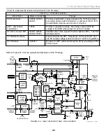
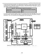
Chart 21-2 explains the function of each block in the HV stage.
Chart 21-2 - HV Block Operation
Block Name
Major component
Purpose
PWM Generator
IC8008, Q8035,
Q9035
Provides regulated B+ supply voltage to the HV Output stage,
preventing picture width fluctuations. A sample of the HV from
the distribution block is used for error correction
LOT – Low Output
Transformer
T8004
Primary is regulated voltage. Secondary outputs 200V B+
voltage to the RGB video output ICs on the C boards.
HV Drive / Output, FBT
Q8005, Q8032,
Q8038, T8005
Amplifies the H drive signal to feed the flyback (FBT). The FBT
develops the HV.
HV Distribution Block
Input is HV from the FBT. Outputs are HV for each CRT and
one HV sample voltage reduced to about 7.4Vdc for regulation .
HV Protection
IC8006-7
Monitors the FBT output and stops the HV by grounding out the
H Drive input.
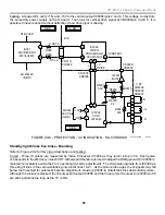
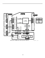
Refer to Figure 21-2 for the operational description of the HV stage.
FIGURE 21-2 - HIGH VOLTAGE STAGE - RA-5 CHASSIS
T8005
FBT
IC8007
PROT. 1
Q8028-9
ABL
DRIVER
Q8004
Q8016
Q8019
Q8020
H DRIVE
Q8023
H OUT
REG.
Q8027
DRIVER
Q8036
Q8037
IC8008
PWM GEN.
1
10
3
3
C8118
LOT
T8004
1
14
12
12
1
6
2
2
4
1
HV BLK
7
VIDEO
OUT B+
C B BD.
14
10
10
9
IC3006
VIDEO
PROCESS
40
7
3
5
IC8006
PROT. 2
5
3
2
D8025
D8023
+12V
CN8016
CRT
HV
R8171
100
+135V
D8036
15V
MIX OUT TO
IC8007
Q8035
HV REG.
P
CH
CN6106/
CN8013
CN8004/
CN3005
CN3007/
CN8006
V BD.
VEL MOD COILS
CN3023/
CN9001
CN3010/
CN9001
CN3001/
CN9001
+135V
SEC.P.S
IC6001
(G BD.)
D8039
200V
R8219
D8038
R8223
CN8022/
CN7304
D8029
D8030
C8142
ABL
R
R8153
PROT.
VR8002
100k
D8017
N
D8031
18V
D8034
D8035
R8160
R8198
10k
Q8021
Q8022
DRIVERS
Q8005,
Q8032
+15V
CN8021
A BD.
G BD.
D BD.
Q8038
HV OUT
D BD.
+135V
+135V
8/31/01
34TVP12 1350
1
1
1
200V TO
R8196
8.1V
7.46VDC
7
11
S
D
G
D8015
LATCH
18
6
VR8001
5k
HV
1
1
Summary of Contents for KD-34XBR2 - 34" Hdtv Fd Trinitron Wega
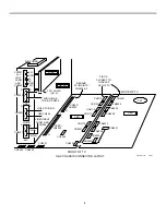
Page 77: ...74 RA 5A Chassis Board Layout ...
Page 108: ...APPENDIX ...

