97
21. RA-5A Chassis High Voltage Stage
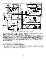
PWM Regulator
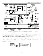
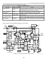
This stage controls the HV level by regulating the B+ voltage from Q8035. IC8008 starts when both 12Vdc and H
drive pulses are input to pins 1 and 14 respectively. Pulses are output pin 3. The width of the pulse is dependent
upon the error voltage input IC8008/pin 12. The higher the input voltage, the narrower the low going output
pulses.
The pulses are amplified by P channel MOSFET Q8035 and applied to the primary winding of LOT T8004/pin 7.
Typical voltage output from Q8035/drain = 130Vdc. The other end of this primary winding at pin 1 goes to HV
Output Transistor Q8038/collector to develop HV. The secondary of LOT T8004 makes 200V for the RGB output
drivers on the C boards (unrelated to the HV development but linked to maintain picture brightness uniformity).
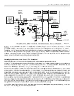
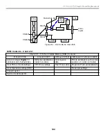
HV Drive / Output, FBT
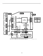
This stage is located in Figure 21-2 below the PWM Regulator stage. It begins by amplifying the 33kHz horizontal
drive signal from Video Process IC3006/pin 40 in various stages and uses the final amplified signal from Q8038
to drive the flyback transformer T8005. The flyback steps up the input voltage to HV level and the HV distribution
block (external to the D board) sends the voltage to the three picture tubes. Another secondary winding of T8005/
pin 6 produces a low voltage that represents the FBT output. This output is rectified by D8038 and used in the HV
protection circuit.
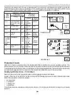
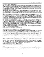
Q8038 is a new device used in this TV set. It tests like an enhancement N channel MOSFET. Normally, all leads
measure infinity resistance to each other. If you charge the base/gate lead, then connect the oh to the
collector/drain, a resistance will appear for over an hour if the gate lead is not touched.
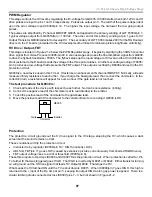
The test procedure for Q8038 is:
1. Check all leads of the device with respect to each other. Normal is no resistance (infinity).
2. Connect the negative lead of the ohmmeter (set to read diodes) to the emitter.
3. Touch the positive lead of the ohmmeter to the gate/base lead.
4. Move the positive lead of the ohmmeter to the collector/drain for a reading if Q8038 is OK.
Q8038
Emitter
Gate
Collector
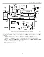
Protection
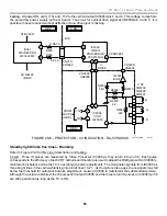
The protection circuit grounds out the H drive signal to the HV stage, stopping the HV, which causes a dark
screen but the sound remains normal.
These conditions will trip the protection circuit:
●
Instructed to by regulator IC8008/pin 10 = HIGH (normally LOW).
●
ABL from FBT/pin 11 goes LOW (caused by excessive pix tube current usually from shorted RGB Drivers).
●
FBT output voltage rises to a critical threshold (T8005/pin 6).
These three inputs to Op Amps IC8006 and IC8007 form the protection circuit. When protection is called for, Pin
7 of either IC that was triggered goes HIGH. The HIGH is inverted by Q8021 or Q8022. Either transistor turning
on will ground out the H Drive signal that feeds HV Output Q8038. That stops the HV.
What keeps the HV latched ON until the TV is shut down is D8015. When IC8006/pin 7 goes HIGH, this high is
returned to the + input of the Op Amp at pin 3, keeping its output HIGH as long as power is applied. There is a
similar latching diode connected across IC8007/pins 7 – 3 but not shown in Figure 21-2.
Summary of Contents for KD-34XBR2 - 34" Hdtv Fd Trinitron Wega
Page 77: ...74 RA 5A Chassis Board Layout ...
Page 108: ...APPENDIX ...


