ECC0
ECC1
ECC2
ECC3
Control0
Transmit0
ECC0
Status0
Receive0
Control1
Transmit1
ECC1
Status1
Receive1
Control2
Transmit2
ECC2
Status2
Receive2
Control3
Transmit3
ECC3
Status3
Receive3
Control126
Transmit126
ECC126
Status126
Receive126
Control127
Transmit127
ECC127
Status127
Receive127
ECC126
ECC127
Buffer 0
1
2
3
...
126
127
0
15
16
31
32
38
0
15
16
31
32
38
Optional
Optional
Parity0
Parity1
Parity2
Parity3
Control0
Transmit0
Parity0
Status0
Receive0
Control1
Transmit1
Parity1
Status1
Receive1
Control2
Transmit2
Parity2
Status2
Receive2
Control3
Transmit3
Parity3
Status3
Receive3
Control126
Transmit126
Parity126
Status126
Receive126
Control127
Transmit127
Parity127
Status127
Receive127
Parity126
Parity127
Buffer 0
1
2
3
...
126
127
0
15
16
31
32
35
0
15
16
31
32
35
Optional
Optional
TXRAM Bank
RXRAM Bank
Multi-buffer RAM
1605
SPNU563A – March 2018
Copyright © 2018, Texas Instruments Incorporated
Multi-Buffered Serial Peripheral Interface Module (MibSPI) with Parallel Pin
Option (MibSPIP)
28.4 Multi-buffer RAM
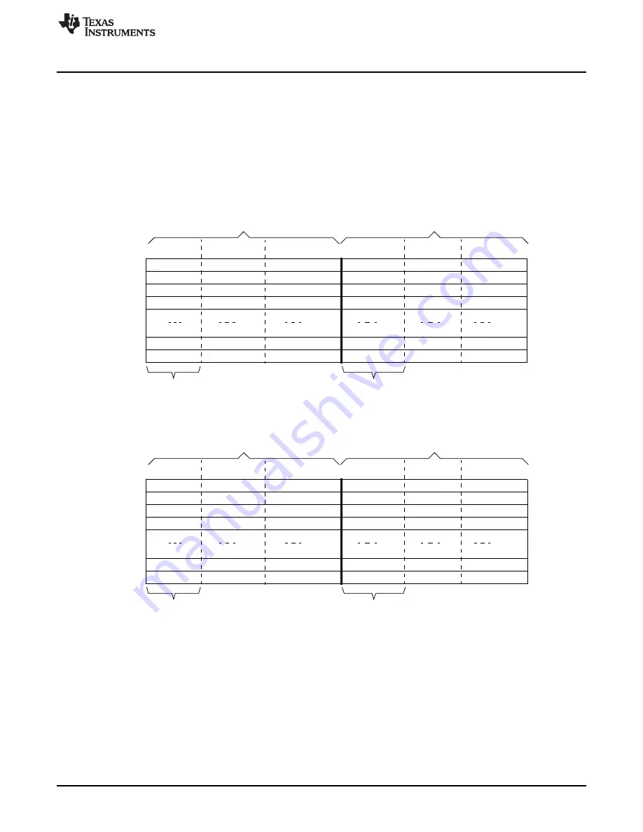
The multi-buffer RAM comprises of all buffers, which can be configured identically. The multi-buffer RAM
contains two banks of up to128/256 words of 32 bits for a maximum configuration, one each for TXRAM
(replicating the SPIDAT1 register) and RXRAM (replicating the SPIBUF register). The buffers can be
partitioned into multiple transfer groups, each containing a variable number of buffers. Each of the buffers
can be sub-divided into a 16-bit transmit field, a 16-bit receive field, a 16-bit control field, and a 16-bit
status field. A 4-bit parity field per word is also included in each RAM bank, as shown in
. If
ECC support is implemented for RAM fault detection, then a 7-bit ECC field per word is also included in
each RAM bank, as shown in
Figure 28-86. Multi-buffer RAM Configuration When Parity Check is Supported
Depth will be up to 256 buffers, if EXTENDED_BUF feature is implemented.
Figure 28-87. Multi-buffer RAM Configuration When ECC Check is Supported
Depth will be up to 256 buffers, if EXTENDED_BUF feature is implemented.
All fields can be read and written with 8-bit, 16-bit, or 32-bit accesses.
The transmit fields can be written and read in the address range 000h to 1FFh. The transmit words
contain data and control fields.
The receive RAM fields are read-only and can be accessed through the address range 200h to 3FCh. The
receive words contain data and status fields.
The chip select number bit field CSNR[7:0] of the control field for a given word is mirrored into the
corresponding receive-buffer status field after transmission.
The Parity is automatically calculated and copied to Parity location


