


Theory of Operation—492/492P Service Vol. 1 (SN B030000 & up)
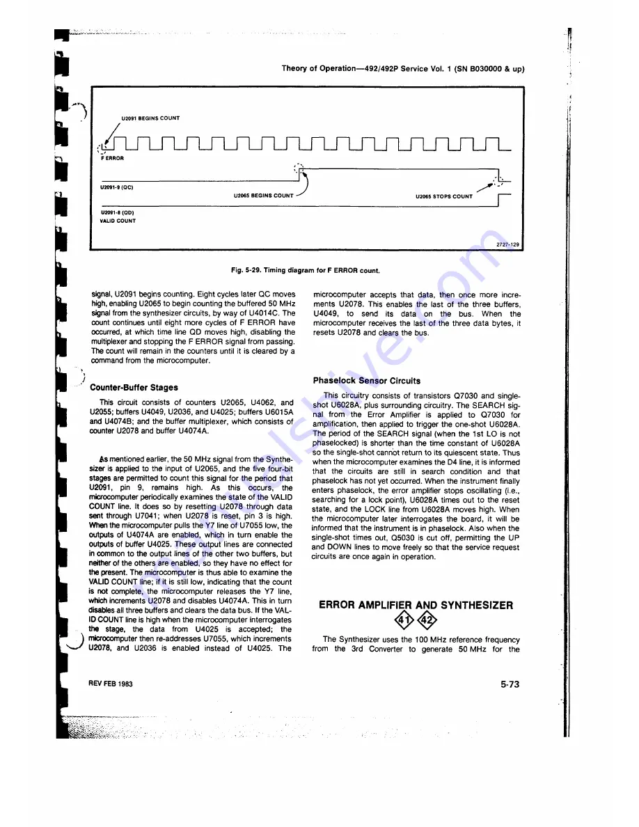
Fig. 5-29. Timing diagram for F ERROR count.
signal, U2091 begins counting. Eight cycles later QC moves
high, enabling U2065 to begin counting the buffered 50 MHz
signal from the synthesizer circuits, by way of U4014C. The
count continues until eight more cycles of F ERROR have
occurred, at which time line QD moves high, disabling the
multiplexer and stopping the F ERROR signal from passing.
The count will remain in the counters until it is cleared by a
command from the microcomputer.
Counter-Buffer Stages
This circuit consists of counters U2065, U4062, and
U2055; buffers U4049, U2036, and U4025; buffers U6015A
and U4074B; and the buffer multiplexer, which consists of
counter U2078 and buffer U4074A.
As mentioned earlier, the 50 MHz signal from the Synthe
sizer is applied to the input of U2065, and the five four-bit
stages are permitted to count this signal for the period that
U2091, pin 9, remains high. As this occurs, the
microcomputer periodically examines the state of the VALID
COUNT line. It does so by resetting U2078 through data
sent through U7041; when U2078 is reset, pin 3 is high.
When the microcomputer pulls the Y7 line of U7055 low, the
outputs of U4074A are enabled, which in turn enable the
outputs of buffer U4025. These output lines are connected
in common to the output lines of the other two buffers, but
neither of the others are enabled, so they have no effect for
the present. The microcomputer is thus able to examine the
VALID COUNT line; if it is still low, indicating that the count
is not complete, the microcomputer releases the Y7 line,
which increments U2078 and disables U4074A. This in turn
disables all three buffers and clears the data bus. If the VAL
ID COUNT line is high when the microcomputer interrogates
the stage, the data from U4025 is accepted; the
microcomputer then re-addresses U7055, which increments
U2078, and U2036 is enabled instead of U4025. The
microcomputer accepts that data, then once more incre
ments U2078. This enables the last of the three buffers,
U4049, to send its data on the bus. When the
microcomputer receives the last of the three data bytes, it
resets U2078 and clears the bus.
Phaselock Sensor Circuits
This circuitry consists of transistors Q7030 and single
shot U6028A, plus surrounding circuitry. The SEARCH sig
nal from the Error Amplifier is applied to Q7030 for
amplification, then applied to trigger the one-shot U6028A.
The period of the SEARCH signal (when the 1 st LO is not
phaselocked) is shorter than the time constant of U6028A
so the single-shot cannot return to its quiescent state. Thus
when the microcomputer examines the D4 line, it is informed
that the circuits are still in search condition and that
phaselock has not yet occurred. When the instrument finally
enters phaselock, the error amplifier stops oscillating (i.e.,
searching for a lock point), U6028A times out to the reset
state, and the LOCK line from U6028A moves high. When
the microcomputer later interrogates the board, it will be
informed that the instrument is in phaselock. Also when the
single-shot times out, Q5030 is cut off, permitting the UP
and DOWN lines to move freely so that the service request
circuits are once again in operation.
ERROR AMPLIFIER AND SYNTHESIZER
< > < § >
The Synthesizer uses the 100 MHz reference frequency
from the 3rd Converter to generate 50 MHz for the
REV FEB 1983
5-73


