Copyright © Siemens AG 2016. All rights reserved
238
ERTEC 200P-2 Manual
Technical data subject to change
Version
1.0
2.3.9.2.2
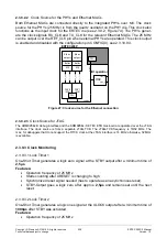
Clock Source for the PHYs and Ethernet MACs
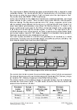
Both Ethernet MACs are connected directly to the integrated PHYs over MII. The clock
source for the PHYs (25 MHz) is from the quartz oscillator on the PHY die. This clock also
functions as the input clock for the ERTEC die (see 2.3.9.2, Figure 74). The PHYs gener-
ate the clock signals RX_CLK and TX_CLK for the relevant Ethernet MACs. The 25 MHz
can be output over the REF_CLK pin when external PHYs are operated. This clock output
is enabled and disabled with the configuration pin CONFIG(0), see 2.3.10.9.3
PHY0
(MII)
PHY1
(MII)
Ether-
net port
Buffer
MII
Ether-
net port
Buffer
MII
MII operation
ERTEC200P
CLKP_A
OSC
CLKP_B
25MHz
PLL
PLL
Figure 27:
Clock source for the Ethernet connection
2.3.9.2.3
Clock Source for JTAG
The ARM926EJ-S debug interface and the ARM926EJ-S ETM / ETB macrocell are operated over the JTAG
interface. The clock source is from a separate JTAG-TCK. The JTAG-TCK frequency is 16/32 MHz. The
max. for debuggers that do not support the RTCK clock at the JTAG interface is 16 MHz; otherwise, 32 MHz
is available.
2.3.9.3 Clock Monitoring
2.3.9.3.1 Lock Timer 1
One-Shot Timer generates a logic zero signal at the STBY output after a minimum time of
2,5µs
.
Features:
Operation frequency of 25 MHz
Starts counting after XRESET is changing to high
Synchronized reset signal needed (has to operate as an asynchronous reset).
STBY-Output goes a logic zero after approx.
2,5µs
and remains set until the next
reset.
2.3.9.3.2 Lock Timer 2
One-Shot Timer generates a logic one signal at the XLOCK output after a minimum time of
1000µs
after STBY was activated.
Features:
Operation frequency of 25 MHz


