Copyright © Siemens AG 2016. All rights reserved
27
ERTEC 200P-2 Manual
Technical data subject to change
Version 1.0
2.3.1.3 ARM926EJ-S processor
ARM926EJ-S revision r0p5 contains an ARM9E-S processor core with Harvard architec-
ture. Unlike the ARM9 processor core of ARM9TDMI, this processor core has the im-
proved
v5TE
architecture. The main improvements relate to ARM/thumb interworking
(faster switching between ARM and thumb code segments) and an improved multiplier
structure. Alongside the processor core, ARM9E-S also includes embedded ICE logic RT.
This logic is controlled by the integrated JTAG interface. Document /9/ (see chapter 7.2)
detail the connection of the embedded ICE interface connector to ERTEC 200P (reset,
JTAG connector ...). A detailed description of ARM9E-S can be found in /6/.
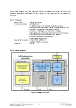
The processor and TCMs (see 5.2.3) can be operated at 125 or 250 MHz. Setting is with
the CONFIG(1) pin (see 2.3.10.9.3). The AHB interfaces always operate at 125 MHz
.
Important: ARM926EJ-S can only be operated in little-endian mode.
The following bit must be set for the ARM926EJ-S core to detect unaligned access:
CP15 register c1 (Control Register), set bit 1 (A-bit) to enable fault checking of ad-
dress alignment.
2.3.1.3.1 Cache structure of ARM926EJ-S
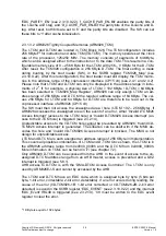
The functional scope of the ARM926 cache has the following features:
- 16 KByte of instruction cache
- 16 KByte data cache
- Write buffer for data cache write back function
- Caches are 4-way set associative caches with 1-KByte segments
- One segment consists of 32 lines and each line contains 32 bytes (i.e. 8 words).
The content of the cache segments can be "locked". This lock function makes it possible
permanently to retain the instruction set for fast routines in the I-cache. In ARM926EJ-S,
this mechanism can only be implemented on a segment-specific basis. More information
on caching can be found in /7/ (see chapter 7.2
If a QVZ interrupt occurs during an I-cache refill following an AHB error (caused for ex-
ample by a WRAP8 at the end of the memory), no Prefetch Abort Exception is triggered
in ARM926EJ-S. The I-cache means that allocation to the erroneous word is no longer
possible for the ARM. However, it is advisable to configure the MMU so that an
ARM926EJ-S exception is generated in this case. An MMU exception is then triggered
when you leave the memory area.
The I-cache and D-cache have one byte of parity. The I-tag and D-tag RAM is also parity-
protected. If an error occurs when reading the I-cache or the relevant I-tag entry, the
cause of the error (I_Cache_Parity, I_Tag_Parity) is saved in the SCRB register 'EDC
Event' (see 2.3.10.9.22
X
) and the interrupt 'EDC_Event' IRQ48 is triggered (see 2.3.2.14
).
An error while reading the D-cache or the relevant D-tag entry generates the entry
(D_Cache_Parity, D_Tag_Parity) in the 'EDC Event Register' with the 'EDC_Event' inter-
rupt. '0h' must be written to the EDC event register to clear the error.
The parity bits are undefined after reset. If parity monitoring of the caches is to be used,
the caches must be initialized by the SW (each cache line must be initialized in a loop).
Until this point, the parity logic is disabled. Control is with the SCRB register


