Copyright © Siemens AG 2016. All rights reserved
488
ERTEC 200P-2 Manual
Technical data subject to change
Version
1.0
4.8 Operating Conditions
The supply voltage tolerance includes the supply voltage ripple, i.e. the supply voltage plus
ripple must not exceed the upper limit / violate the lower limit.
4.8.1 Power Up
There is no set order for switches on the supply voltages. However, all must be activated
within a period of 100 ms.
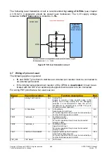
4.8.2 Wiring of CTRL-STBY
To ensure that the outputs remain at high-impedance upon power up (see 00), make sure
that the inputs pins
CTRL_STBY0-2
arein the PCB layout are switched to '0' (GND) during
this time (for example, link to XRESET pin), i.e. that the CTRL_STBY function is active.
Please note that the CTRL_STBY pins control both 3.3 V and 1.8/3.3 V pads.
CTRL_STBY0-2 must
therefore be deactivated
with the corresponding supply voltage
of the controlled IO buffers e.g. operation of the XHIF interface with 1.8 V
deactivation
of CTRL_STBY1, 2 = 1.8 V).
The table below shows which ERTEC 200P IO signals (see 3.2) are controlled with the
CTRL_STBY0-2
input pins:
CTRL_STBY0
(3,3V)
CTRL_STBY1
(1,8V / 3,3V)
CTRL_STBY2
(1,8V /
3,3V)
GPIO31:0
GPIO92
XHIF_D28
GPIO95:93 XHIF_D31-
29
JTAG_RTCK
JTAG_TDO
GPIO79:64 XHIF_D15-0 GPIO91:80 XHIF_D27-
16
GPIO62:46 XHIF_XBE2-0
XHIF_XCS_M
XHIF_XCS_R
XHIF_XRD
XHIF_XWR
XHIF_XIRQ
XHIF_XRDY
XHIF_SEG_2-
0
GPIO63
XHIF_XBE3
P2XTXEN
1)
P2XTXER
1)
P2XTXD0-3
1)
P2XPHYEN
1)
P2XFXMODE
1)
P2XAUTOMDIXEN
1)
P2SDXN
1)
P2SDXP
1)
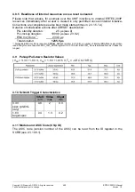
Min.
Max.
Ambient Tempera-
ture
- 40 °C
+ 85 °C
Junction Tempera-
ture
- 40 °C
+ 125 °C
VCC-IO
1,8 V – 10%
1,8 V + 10%
3,3 V – 10%
3,3 V + 10%
Core ERTEC 200P
Die
1,2 V – 0,1V
1,2 V + 0,1V
Core PHY Die
1,5 V – 10%
1,5 V + 10%

