Copyright © Siemens AG 2016. All rights reserved
458
ERTEC 200P-2 Manual
Technical data subject to change
Version
1.0
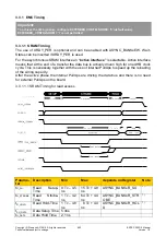
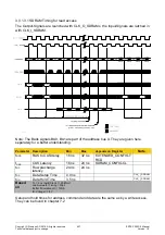
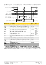
3.3.1.3.2 SDRAM Timing for write access
Note: The Bank signals BA0, BA1 are part of the address bus A. They are given here
separately for a better understanding.
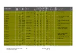
Parame-
ter
Description
Min
Max
depends on Register
No-
te
t
CK
Clock Period
7.8 ns
8.2 ns
-
t
CL
Clock Low Time
3.8 ns
4.2 ns
-
t
CH
Clock High Time
3.8 ns
4.2 ns
-
t
CMS
Command
Setup
Time
3.5 ns
6.6 ns
-
t
CMH
Command Hold Time 1.4 ns
4.5 ns
-
t
AS
Address Setup Time
3.5 ns
6.6
-
t
AH
Address Hold Time
1.4 ns
4.5 ns
-
t
DS
Data Setup Time
3.5 ns
6.6 ns
-
t
DH
Data Hold Time
1.4 ns
4.5 ns
-
t
RCD
RAS to CAS delay
16 ns
40
ns EXTENDED_CONFIG.TRC
D + 1
t
RAS
Row
Address Strobe t
RCD
+ t
WR
1)
t
RC
ROW cycle Time
t
RCD
+ t
WR
+
t
RP
-
-
t
WR
Write to Precharge
Time
16 ns
1)
-
t
RP
Row precharge la- 24 ns
24 ns
-


