Copyright © Siemens AG 2016. All rights reserved
481
ERTEC 200P-2 Manual
Technical data subject to change
Version
1.0
ered feed-back it might have negative
effect on signal reflection. Better
provide a chance to cut the connec-
tion on the target (jumper or solder
bridge) in case problems arise.
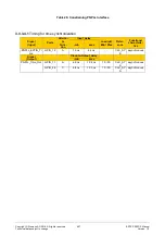
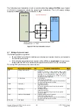
TCK
In
Pulldown
not necessary
4k7 Pulldown
4k7 Pulldown
You should place a pull-up or pull-
down resistor (1k - 47k) on this line in
order to give it a defined state even
when the line is not driven by the
debugger.
TDI
In
-
not necessary
4k7 Pullup
4k7 Pullup
You can place a pull-up or pull-down
resistor (1k - 47k) on this line to
ensure a defined state even when the
line is not driven by the debugger.
TMS
In
Pullup
not necessary
4k7 Pullup
4k7 Pullup
You can place a pull-up or pull-down
resistor (1k - 47k) on this line in order
to give it a defined state even when
the line is not driven by the debugger.
XSRST
In
Pullup
not necessary
because of
internal pullup
not necessary,
because of
internal Pullup
not necessary,
because
internal Pullup
There might be the need to place a
pull-up (1k - 47k) on target side to
avoid unintentional resets when the
debugger is not connected and
probably to strengthen the weak 47k
pull-up in the debug cable.
TDO
out
-
not necessary
not necessary
33Ohm serial
resistor
You can place a 33 series resistor
close to the processor for series
termination. You can place a pull-up
or pull-down resistor (1k - 47k) on this
line.
Note on module development:
To achieve the best possible resistance to interference on the module (see "Circuit for
Production" column in the table above), the XTRST pin on the module must have a
10 KOhm pull-down.
This deactivates JTAG interface during operation, which means that
noise pulses affecting the individual JTAG signals can no longer affect ERTEC 200P func-
tion. If a debugger is used at the JTAG interface, the pull-down has no effect as the de-
bugger actively pulls the XTRST signal to '1'. Only AHB access to the ETM trace buffer
SRAM (ETB, see 2.3.1.3.5 and 3.3.9) is not possible in this configuration.
If access from
an AHB master (e.g. ARM926) to this SRAM (ETB) is required for test purposes, the
XTRST pin requires a 10 KOhm pull-up. Please note that AHB access to the ETM trace
buffer SRAM is only possible in this case if no debugger is connected.
4.6 PHY Wiring
4.6.1 PHY-TX Wiring
Following design hints are recommended for the UTP interface:
RX and TX pairs must be routed 100Ohm differential
Differential length for each pair must match in length
Transformer must be placed as close as possible to the ERTEC 200P
Centre Tap of transformer must be connected with 10Ohm series resistor to
3.3V_Analog.
50Ohm termination resistors must be placed as close as possible to the
ERTEC 200P
An external 12.4kOhm pull down resistor on pin EXTRES must be placed a close as
possible to ERTEC 200P
Analog signals must be placed referenced to analog ground plane or common plane
(same as digital) and must be not coupled with other signals.
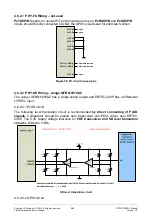
The picture below shows a typical UTP circuit with separate centre taps on the magnetic:

