Copyright © Siemens AG 2016. All rights reserved
164
ERTEC 200P-2 Manual
Technical data subject to change
Version 1.0
2.3.5.5 Timing of the Asynchronous Memory Interfaces
The asynchronous interface can be activated by writing a 1 to the
ADB
bit of the
EXTENDED_CONFIG
register. The data bus is then kept at 1 for one cycle after access.
With pull-up resistors, this speeds up capacity reloading (with wiring). The internal pull-
ups drive the data bus after the active phase. No external pull-ups are therefore required.
For further explanation, SETUP, STROBE and HOLD phases are defined for asynchro-
nous access.
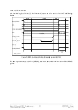
The figures below detail the individual phases in read and write access.
2.3.5.5.1 Read Access
The SETUP phase starts with an active CS signal and ends when the output enable sig-
nal becomes active. The STROBE phase then starts. The STROBE phase lasts until the
output enable signal is deactivated again. This then starts the hold phase. The hold
phase ends when the CS signal is deactivated.
Figure 14: EMC, Notation definition for a read access (ASYNC)
MA
DQM_SDRAM/XBE
MD
XOE_ASYNC
ASYNC_WAIT
SETUP
HOLD
STROBE
ASYNC_read.vsd
XCS_ASYNC
Read Data
DTXR
XOE_DRIVER
111...111
“active interface”
AHB clock cycle

