Copyright © Siemens AG 2016. All rights reserved
31
ERTEC 200P-2 Manual
Technical data subject to change
Version 1.0
More information is available in specifications /4/ and /5/ for the ETM9 cell (see chapter
7.2
X
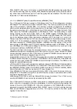
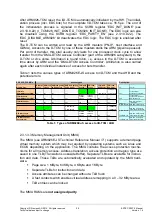
). In addition to these specifications, the following 8 MMD areas have been decoded in
ERTEC 200P with the hardware.
2.3.1.4 Debug Support
2.3.1.4.1 Debug Configuration
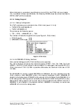
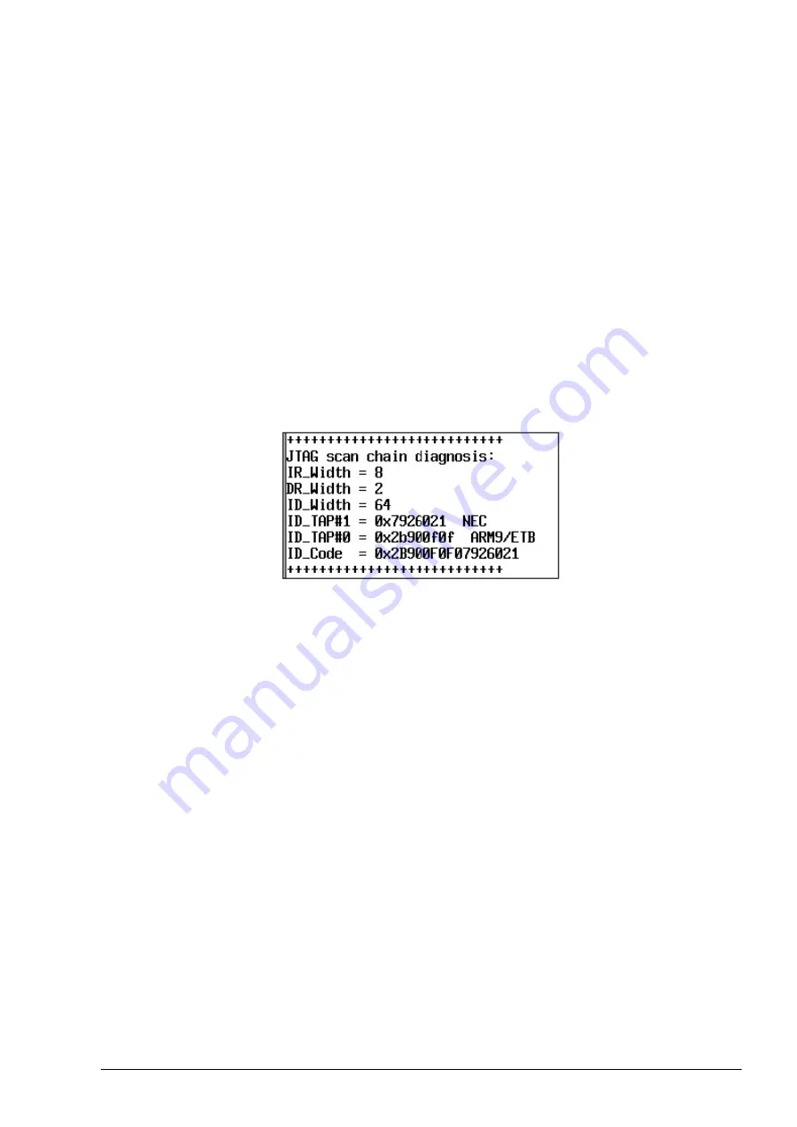
Two TAP controllers are connected in the JTAG chain (see 2.3.1.4.2):
TAP#0: ETB of ARM926EJ-S
TAP#1: ARM926EJ-S
This produces the following queue:
TDI ETB ARM926EJ-S TDO
The number of instruction register bits is (see Figure 6: JTAG chain):
ETB IR length:
4 bits
ARM926EJ-S IR length: 4 bits
Figure 6: JTAG chain
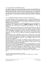
2.3.1.4.2 ARM926EJ-S Debug Interface
Only external debuggers with JTAG interfaces are supported.
The JTAG interface comprises the standard signals (XTRST, TCK, TDI, TMS, TDO and
XSRST). The RTCK clock output is also available. For debuggers that support RTCK, a
JTAG clock rate of TCK = 32 MHz is possible. Otherwise, the maximum clock rate is TCK
=16 MHz.
For ARM926EJ-S, the two signals DBGREQ and DBGACK are also supported over the
JTAG interface. With DBGREQ active, the external debugger forces ARM926EJ-S
straight to the debug state. DBGACK active signals to the debugger that ARM926EJ-S is
in the debug state. Both signals are available as alternate functions at the GPIO31-0 pins.
Before these debug signals can be used, they must be enabled in the GPIO31-0 block. If
DBGREQ is not enabled in its alternate function, DBGREQ is internally not active and
ARM926EJ-S is not in the debug state.

